EN25F20 데이터 시트보기 (PDF) - Eon Silicon Solution Inc.
부품명
상세내역
일치하는 목록
EN25F20 Datasheet PDF : 33 Pages
| |||
EN25F20
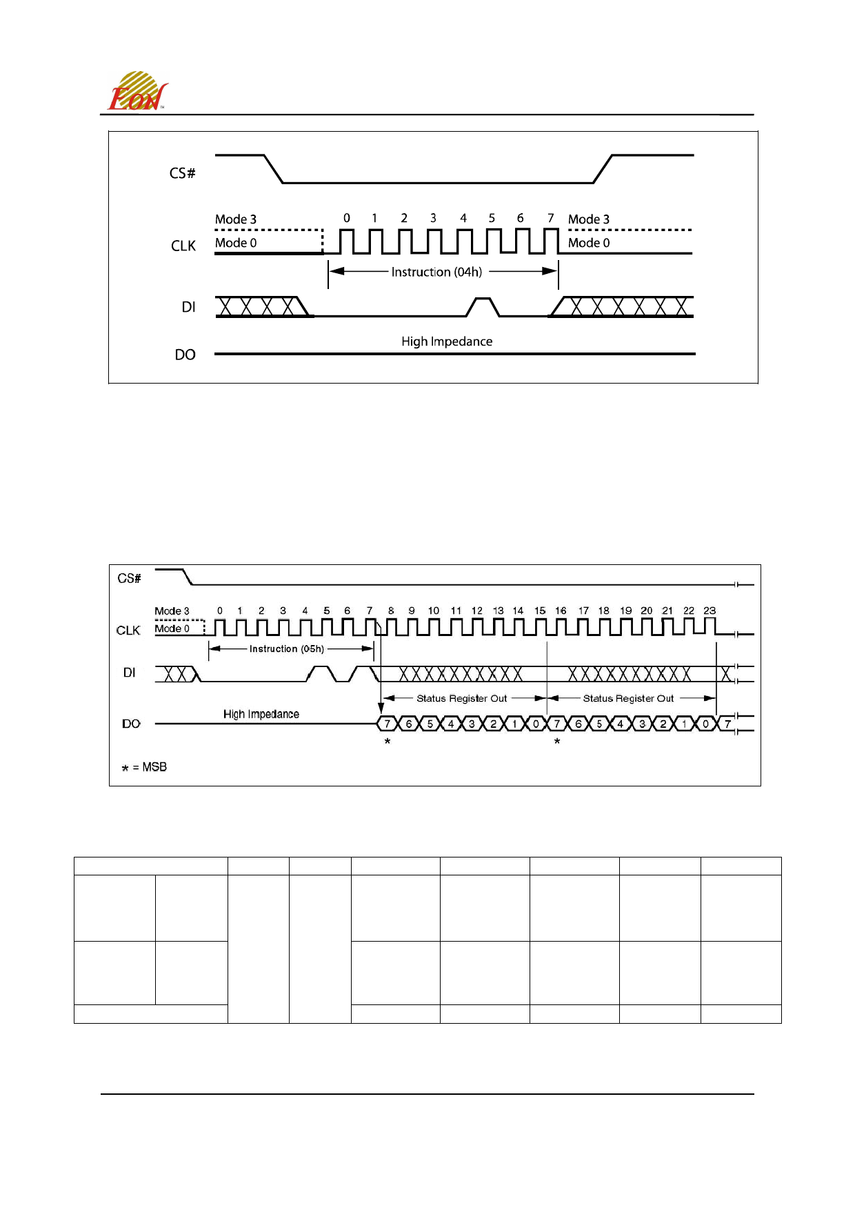
Figure 6. Write Disable Instruction Sequence Diagram
Read Status Register (RDSR) (05h)
The Read Status Register (RDSR) instruction allows the Status Register to be read. The Status
Register may be read at any time, even while a Program, Erase or Write Status Register cycle is in
progress. When one of these cycles is in progress, it is recommended to check the Write In Progress
(WIP) bit before sending a new instruction to the device. It is also possible to read the Status Register
continuously, as shown in Figure 7.
Figure 7. Read Status Register Instruction Sequence Diagram
Table 6. Status Register Bit Locations
S7
S6
S5
S4
S3
S2
S1
S0
SRP OTP_LOCK
Status Register
bit
Protect
(note 1)
BP2
BP1
BP0
WEL
WIP
(Block Protected (Block Protected (Block Protected (Write Enable (Write In
bits)
bits)
bits)
Latch)
Progress bit)
1 = status
register write
disable
1 = OTP
sector is
protected
Reserved Reserved
bits
bits
(note 2)
(note 2)
(note 2)
1 = write
enable
0 = not write
enable
1 = write
operation
0 = not in write
operation
Non-volatile bit
Non-volatile bit Non-volatile bit Non-volatile bit volatile bit
volatile bit
Note
1. In OTP mode, SRP bit is served as OTP_LOCK bit.
2. See the table “Protected Area Sizes Sector Organization”.
This Data Sheet may be revised by subsequent versions
11
or modifications due to changes in technical specifications.
©2004 Eon Silicon Solution, Inc.,
Rev. E, Issue Date: 2008/12/15
www.eonssi.com
Share Link: 