EN25F05 데이터 시트보기 (PDF) - Eon Silicon Solution Inc.
부품명
상세내역
일치하는 목록
EN25F05 Datasheet PDF : 31 Pages
| |||
EN25F05
Write Enable (WREN) (06h)
The Write Enable (WREN) instruction (Figure 5) sets the Write Enable Latch (WEL) bit. The Write
Enable Latch (WEL) bit must be set prior to every Page Program (PP), Sector Erase (SE), Block
Erase (BE), Chip Erase (CE) and Write Status Register (WRSR) instruction.
The Write Enable (WREN) instruction is entered by driving Chip Select (CS#) Low, sending the
instruction code, and then driving Chip Select (CS#) High.
Figure 5. Write Enable Instruction Sequence Diagram
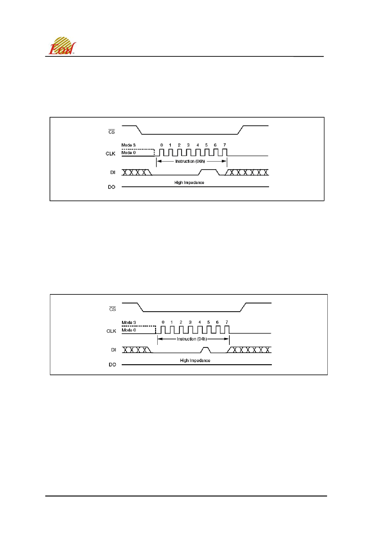
Write Disable (WRDI) (04h)
The Write Disable instruction (Figure 6) resets the Write Enable Latch (WEL) bit in the Status
Register to a 0 or exit from OTP mode to normal mode. The Write Disable instruction is entered by
driving Chip Select (CS#) low, shifting the instruction code “04h” into the DI pin and then driving Chip
Select (CS#) high. Note that the WEL bit is automatically reset after Power-up and upon completion
of the Write Status Register, Page Program, Sector Erase, Block Erase (BE) and Chip Erase
instructions.
Figure 6. Write Disable Instruction Sequence Diagram
Read Status Register (RDSR) (05h)
The Read Status Register (RDSR) instruction allows the Status Register to be read. The Status
Register may be read at any time, even while a Program, Erase or Write Status Register cycle is in
progress. When one of these cycles is in progress, it is recommended to check the Write In
Progress (WIP) bit before sending a new instruction to the device. It is also possible to read the
Status Register continuously, as shown in Figure 7.
This Data Sheet may be revised by subsequent versions
9
or modifications due to changes in technical specifications.
©2004 Eon Silicon Solution, Inc., www.essi.com.tw
Rev. B, Issue Date: 2008/06/23
Share Link: 