EM4069A5CI2LC 데이터 시트보기 (PDF) - EM Microelectronic - MARIN SA
부품명
상세내역
일치하는 목록
EM4069A5CI2LC
EM Microelectronic - MARIN SA

EM4069A5CI2LC Datasheet PDF : 15 Pages
| |||
EM4069
EM4169
Timing Characteristics
VDD = 3.0 V, VSS = 0 V, fCOIL1 = 125 kHz square wave, VCOIL1 = 5V, TOP = 25°C, unless otherwise specified
Parameter
Option : 64 RF periods per bit
Read bit period
EEPROM write time
Synchronization pattern phase 1
Synchronization pattern phase 2
Synchronization pattern phase 3
Symbol Condition
tRDB
tWee
tS1
tS2
tS3
Min. Typ.
64
20
4.1
1.5
1.5
Max.
5.0
2.0
4.0
Unit
RF periods
ms
ms
ms
ms
Option : 32 RF periods per bit
Read bit period
tRDB
EEPROM write time
tWee
Synchronization pattern phase 1
tS1
Synchronization pattern phase 2
tS2
Synchronization pattern phase 3
tS3
32
20
2.1
0.8
0.8
RF periods
ms
2.5
ms
1.0
ms
2.0
ms
RF periods represent periods of the carrier frequency emitted by the transceiver unit.
See figure 12 for Synchronization pattern phases.
Due to amplitude modulation of the coil-signal, the clock-extractor may miss clocks or add spurious clocks close to
the edges of the RF-envelope. This desynchronization will not be larger than ± 3 clocks per bit and must be taken into
account when developing reader software.
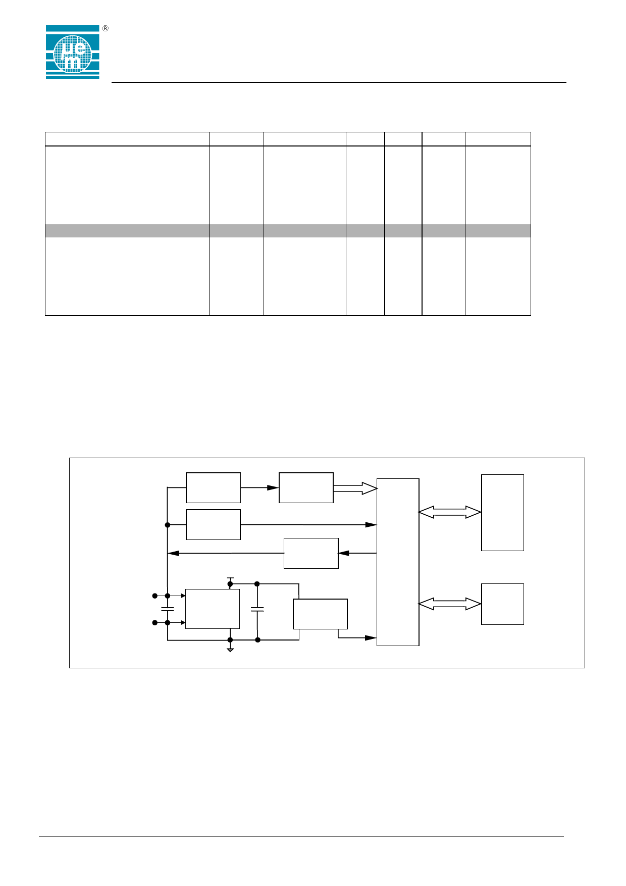
Block Diagram
COIL1
CR
VSS
Clock
Extractor
Sequencer
Data
Extractor
VDD
Modulator
Power
Supply
Cbuf
VSS
Power on
Reset
Reset
Control
Logic
EEPROM
ROM
Fig. 3
Copyright 2003, EM Microelectronic-Marin SA
3
www.emmicroelectronic.com
Share Link: