EM4069B6WW11E 데이터 시트보기 (PDF) - EM Microelectronic - MARIN SA
부품명
상세내역
일치하는 목록
EM4069B6WW11E
EM Microelectronic - MARIN SA

EM4069B6WW11E Datasheet PDF : 15 Pages
| |||
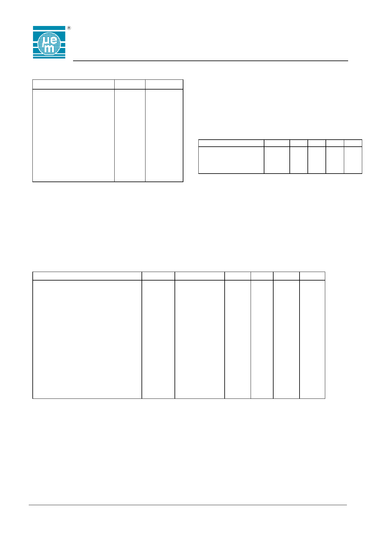
Absolute Maximum Ratings
VSS = 0V
Parameter
Symbol
Power supply
VDD
Input Voltage (pads TST,
TCP, TIO)
VPIN
Input current on COIL1
Input voltage on COIL1
ICOIL1
VCOIL1
Storage temperature
Electrostatic discharge to
MIL-STD-883C method 3015
TSTORE
VESD
Conditions
-0.3 to +5.5V
- 0.3 to
VDD+0.3V
-30 to
+30mA
-10 to +10V
-55 to
+125°C
1000V
Stresses above these listed maximum ratings may cause
permanent damage to the device. Exposure beyond
specified electrical characteristics may affect device
reliability or cause malfunction.
Electrical parameters and functionality are not
guaranteed when the circuit is exposed to light.
EM4069
EM4169
Handling Procedures
This device has built-in protection against high static
voltages or electric fields. However due to the unique
properties of this device, anti-static precautions should
be taken as for any other CMOS component. Unless
otherwise specified, proper operation can only occur
when all terminal voltages are kept within the supply
voltage range.
Operating Conditions VSS = 0V
Parameter
Symbol Min.
Operating temperature
AC voltage on coil 1
Maximum coil current
Frequency on coil 1
TOP
VCOIL1
ICOIL1
FCOIL1
-40
-10
100
Typ.
+25
*
125
Max. Units
+85 °C
Vpp
10 mA
150 kHz
*) Maximum voltage is defined by forcing 10mA on
Coil1 – Vss
Electrical Characteristics
Unless otherwise specified: VDD= 1.0V to 5.5V, TA=-40 to +125°C.
Parameter
Symbol Condition
Regulated Supply Voltage
Reg. Voltage reading EEPROM (note 3)
Supply current in read mode
Reg. Voltage writing EEPROM
Supply current write mode
Power Check Voltage
Modulator ON voltage drop
Modulator ON voltage drop
POR level
Clock extractor
Peak detector threshold.
Peak detector hysteresis
Resonance capacitor (note 1)
EEPROM data retention (note 2)
EEPROM write cycles
VDD
VRD
IRD
VWR
IWR
VPC
Von1
Von2
VPOR
VCOIL1
Vpd
Vpdh
CR
TRET
NCY
ICOIL1 = 10mA
VDD = 3.5 V
ICOIL1 = ±100µA
ICOIL1 = ±1 mA
Rising edge
VDD = 3.3 V
VDD = 3.3 V
32 kHz, 0.3Vpp
TOP = 55°C
VDD = 3.6 V
Note 1:
Note 2:
Note 3:
Value of the resonance capacitor may vary in limits of ± 12%
Statistics show a variation of capacitance within one lot of ± 5%.
These figures are given as information only.
Based on 1000 hours at 150°C.
VRD must be higher than VPOR Level.
Min.
3.0
2.0
2.5
2.4
1.2
3
1.5
0.5
3.2
20
10
100000
Typ.
3.5
3.8
50
2.8
1.45
3.6
1.85
4
100
78
Max.
4.0
5,5
100
3.15
1.75
4.5
2.20
4.6
200
Units
V
V
µA
V
µA
V
V
V
V
VPP
VPP
mV
pF
years
cycles
Copyright 2003, EM Microelectronic-Marin SA
2
www.emmicroelectronic.com
Share Link: