EM4056 데이터 시트보기 (PDF) - EM Microelectronic - MARIN SA
부품명
상세내역
일치하는 목록
EM4056
EM Microelectronic - MARIN SA

EM4056 Datasheet PDF : 14 Pages
| |||
EM4056
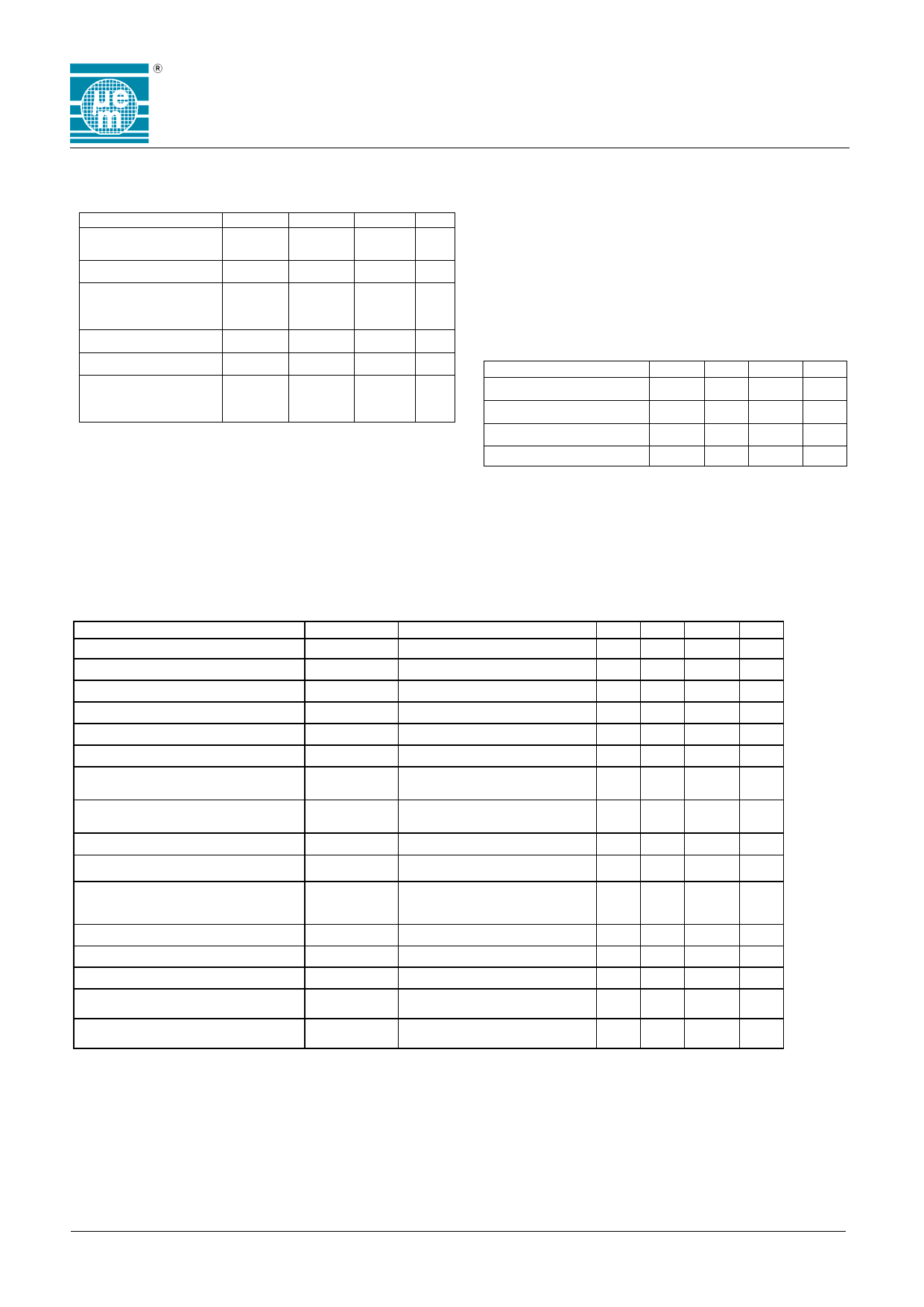
Absolute Maximum Ratings
Parameter
Voltage on Power
Supply pads
Voltage on other pads
Max. AC peak current
induced on COIL1 and
COIL2
Storage temperature
Operating temperature
Electrostatic discharge
max. to MIL-STS-883C
method 3015
Symbol
VDD
VPAD
ICOIL
TSTORE
TOP
VESD
Min.
-0.3
Max.
6.0
Units
V
VSS - 0.3 VDD+ 0.3 V
- 30
+ 30 mAp
-55
+125 oC
-40
+85
oC
1000
V
Stresses above these listed maximum ratings may cause
permanent damages to the device. Exposure beyond
specified operating conditions may affect device reliability
or cause malfunction.
Handling Procedures
This device has built-in protection against high static
voltages or electric fields; however, anti-static precautions
must be taken as for any other CMOS component. Unless
otherwise specified, proper operation can only occur when
all terminal voltages are kept within the voltage range.
Unused inputs must always be tied to a defined logic
voltage level.
Operating Conditions
Parameter
Max. AC Voltage on COIL
Max. AC coil current
Carrier frequency
Operating temperature
Symbol Min
VCOIL
ICOIL -10
fCOIL 100
TOP -40
Max Units
(Note 1) Vpp
+10 mAp
150 kHz
+85
°C
Note 1: Defined by forcing 10mA on Coil1-Coil2
Electrical Characteristics
Unless otherwise specified : VDD = 4.0 V, VSS = 0 V, TOP = 25°C, VCOIL = 4.5 Vpp, fCOIL = 125 KHz Sine wave
Parameter
Symbol
Conditions
Min Typ Max Unit
Supply voltage (not regulated)
VPOS-REG
(Note1) V
Supply voltage (regulated)
VDD
VPOS-REG = max (note 1)
3.4
4.3 V
Min. EEPROM Read voltage
VRD
Read mode (note 2)
2.5
V
Min. EEPROM Write voltage
VWR
Write mode
2.5
V
EEPROM Read current
IRD
Read mode
19 25 µA
EEPROM Write current
IWR
Write mode
60 80 µA
Power check EEPROM write
current
IPWCHK VDD = 4.0 V
70 95 µA
EEPROM pwr check threshold
voltage
VPWCHK
2.52 2.75 3.10 V
EEPROM data endurance
NCY
Erase all / Write all
105
cycle
EEPROM retention (note 3)
TRET
TOP = 55oC after 105 cycles 10
year
Voltage drop VCOIL- VSS on
modulator
VON
ICOIL = 100 µA
ICOIL = 5 mA
0.50 V
2.50 V
Resonance capacitor
CCOIL
330 340 350 pF
POR voltage (high)
VPRH
VDD rising
2.0 2.6 V
MONOFLOP delay
TMONO
25 50 85 µs
Min. voltage of clock extractor 1 VCLK1min
(note 4)
Vcoil1-coil2 (min for extraction)
4.5 Vpp
Min. voltage of clock extractor 2 VCLK2min Vcoil1-coil2 (min for extraction)
(note 5)
1.0 Vpp
Note 1: Max. supply voltage (not regulated) is defined by forcing a DC current 10 mAp in pins COIL1-COIL2
Note 2: The circuit is not functional under low level POR voltage
Note 4: Uplink
Note 3: Based on 1000 hours measurement at 150oC
Note 5: downlink
Copyright © 2005, EM Microelectronic-Marin SA
3
www.emmicroelectronic.com
Share Link: