EM4022V14WS11 데이터 시트보기 (PDF) - EM Microelectronic - MARIN SA
부품명
상세내역
일치하는 목록
EM4022V14WS11
EM Microelectronic - MARIN SA

EM4022V14WS11 Datasheet PDF : 15 Pages
| |||
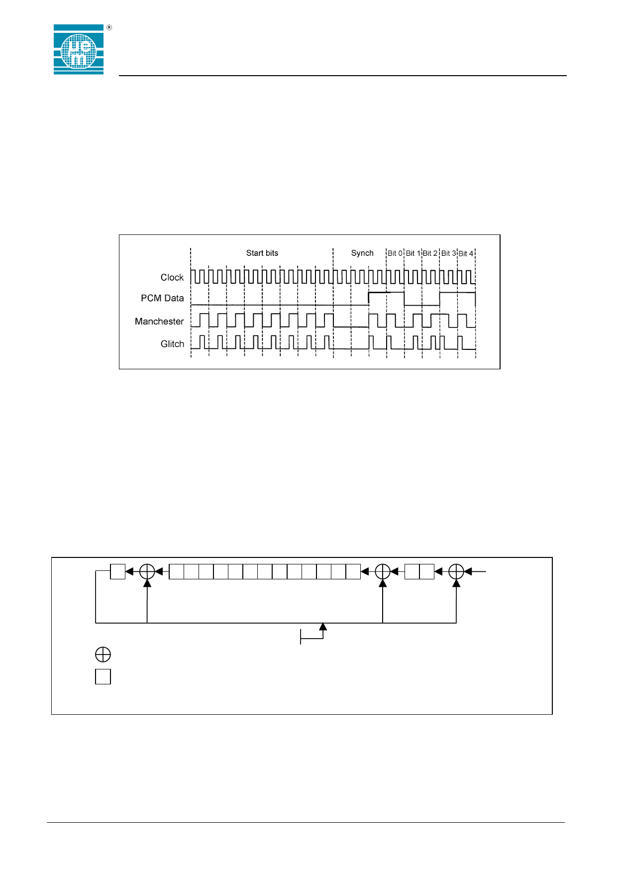
Data Encoder
The transmitted code always consists of an 11 bit
preamble followed by the 64 code bits. The preamble
consists of 8 start bits (ZEROES), followed by a SYNCH.
The SYNCH consists of a LOW for two bit periods
followed by a ONE.
The EM4022 can be programmed for one of two data
encoding methods. The first method is a variation on
Manchester II, i.e. a ONE is represented by a HIGH in
the first half of a bit period, and a ZERO is represented
by a LOW in the first half of a bit period.
Data Encoding
EM4022
The second encoding method is called GLITCH
encoding. A ONE is represented by a HIGH in the first
quarter of the bit period, while a ZERO is represented by
a HIGH in the third quarter of the bit period.
In GLITCH encoding the longest modulation period is
one quarter of a bit period, compared to the Manchester
encoding, where the longest modulation period is one full
bit period. GLITCH encoding therefore requires a much
smaller power storage capacitor.
"0" "0" "1"
Fig. 8
ROM programming
The EM4022 contains three laser fuse ROM blocks that
are pre-programmed by the foundry.
CODE ID ROM
This ROM contains the 64 bit ID code. The foundry will
automatically program a unique 48 bit ID and 16 bit
CRC. In this case the most significant bit of the ID is
programmed into bit 0 of the ROM, which will be
transmitted first.
CONTROL ROM
The operational modes of the EM4022 are pre-
programmed into the CONTROL ROM. The contents of
this one is not read out.
CRC Block Diagram
15
14 13 12 11 10 9 8 7 6 5 4 3 2
MSB
X15
X2
Feedback before shift
Exclusive OR
X Shift Register
CRC-CCITT Generating polynomial = X15 + X2 + X0
10
LSB
X0
Data Input
Fig.9
Copyright 2002, EM Microelectronic-Marin SA
8
www.emmicroelectronic.com
Share Link: