EM4022V13WS11 데이터 시트보기 (PDF) - EM Microelectronic - MARIN SA
부품명
상세내역
일치하는 목록
EM4022V13WS11
EM Microelectronic - MARIN SA

EM4022V13WS11 Datasheet PDF : 15 Pages
| |||
EM4022
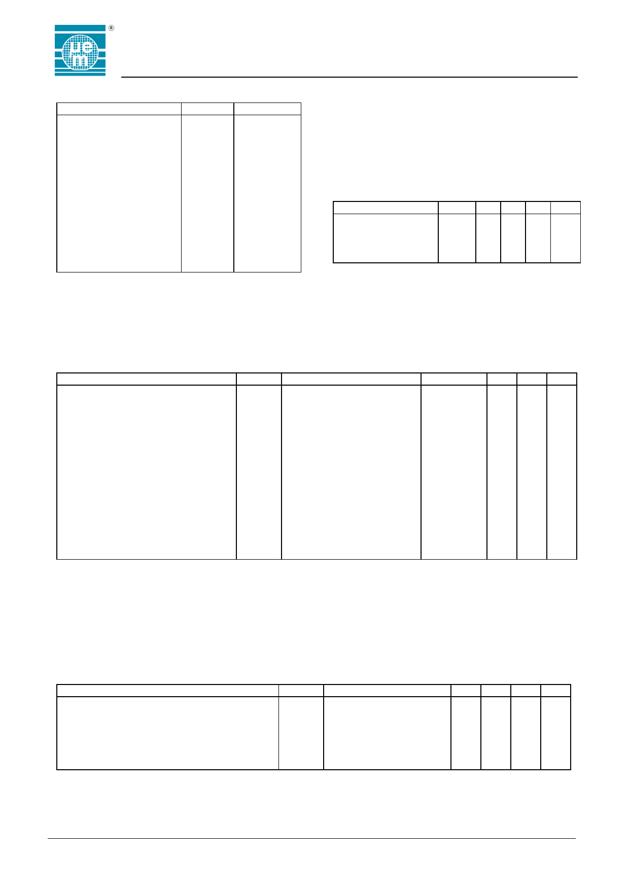
Absolute Maximum Ratings
Parameter
Symbol Conditions
Maximum AC peak current I COIL
induced on COIL1 and
± 30 mA
COIL2
Maximum DC voltage
VM
induced between M and VSS (note1)
Maximum DC current
IM
supplied into M
(note1)
Power supply
VDD - VSS
Max. voltage other pads
Vmax
Min. voltage other pads
Vmax
Storage temperature
TSTORE
Electrostatic discharge
VESD
maximum to MIL-STD-883C
5V
60 mA
-0.3 to VM
VDD + 0.3 V
VSS - 0.3 V
-55 to +125oC
1000 V
method 3015
note1) whatever is reached first
Stresses above these listed maximum ratings may cause
permanent damage to the device. Exposure beyond
specified operating conditions may affect device
reliability or cause malfunction.
Handling Procedures
This device has built-in protection against high static
voltages or electric fields; however, due to the unique
properties of this device, anti-static precautions should
be taken as for any other CMOS component. Unless
otherwise specified, proper operation can only occur
when all the terminal voltages are kept within the supply
voltage range.
Operating Conditions
Parameter
Symbol Min Typ Max Units
Operating temperature TA
-40
+85 oC
Maximum coil current ICOIL -10
10 mA
AC voltage on coil*
VCOIL
15 Vpp
DC voltage on M*
VM
3.5
V
* The AC voltage on the coil and the DC voltage at pad
M are limited by the on-chip shunt regulator loaded at
ICOIL in table 3
Electrical Characteristics
VSUPPLY between 2.0 V and 3.0 V, TA = 25 OC, unless otherwise specified.
Parameter
Symbol Test conditions
Supply voltage (VDD - VSS)
Regulated voltage
Oscillator frequency
Power-on reset threshold
Power-on reset threshold
Power-on reset hysteresis
GAP input time constant
VSUPPLY
VM
FOSC
VPONR
VPONF
VPHYS
TGAP
Modulation transistor ON resistance
Resonance capacitor
Supply capacitor
Current consumption in modulation state
Shunt Regulator current consumption
Gap pull-up current consumption
Dynamic current consumption
RON
CR
CSUP
IMOD
ISHUNT
IGAP
IDYN
IM = 50 mA
VSUPPLY = 3 V
VSUPPLY rising
VSUPPLY falling
Extrapolated with an external
capacitor of 64nF
VSUPPLY = 3 V
f = 100KHz, 100mVpp
f = 100KHz, 100mVpp
VSUPPLY = 2 V
VSUPPLY = 2V
VGAP = 0V, VSUPPLY = 2V
fOSC = 128KHz, VSUPPLY = 2V
Min
Typ
VPONR +100mV
3.3
4
92
125
0.9
1.4
0.7
1.2
80
160
0.4
Max Units
VM
V
4.7 V
160 kHz
1.8 V
1.6 V
240 mV
µs
106.7
6
1.8
3.5
4
8
Ω
110 113.3 pF
140
pF
9 13 µA
200 500 nA
5
7 µA
5 6.5 µA
Timing Characteristics
1) All timings are derived from the on-chip oscillator.
2) The minimum low frequency GAP width for a single chip is 1 bit at its own clock frequency. The reader must however
allow for the spread in clock frequencies possible in a group of tags. Therefore the minimum width of the GAP in MUTE
and WAKE-UP signals must be 1.5 bits. High frequency GAPs can be arbitrarily.
3) The maximum GAP width for a single chip is 6 bits at its own clock frequency. The reader must however allow for the
spread in clock frequencies possible in a group of tags. Therefore the maximum width of the GAP in MUTE and WAKE-UP
signals must be 5 bits.
Parameter
High frequency GAP width
High frequency ACK GAP width
High frequency MUTE and WAKE-UP GAP width
Low frequency ACK GAP width
Low frequency MUTE and WAKE-UP GAP width
GAP separation in WAKE-UP signal
Symbol
THFGAP
W HFACK
W HFMUTE
W LFGAP
W LFACK
W LFMUTE
Test conditions
Min Typ Max Units
50
ns
6 bit
5 bit
1.0 2
6 bit
1.5 2
5 bit
1.5 2
5 bit
Copyright 2002, EM Microelectronic-Marin SA
3
www.emmicroelectronic.com
Share Link: