EM4022 데이터 시트보기 (PDF) - EM Microelectronic - MARIN SA
부품명
상세내역
일치하는 목록
EM4022
EM Microelectronic - MARIN SA

EM4022 Datasheet PDF : 15 Pages
| |||
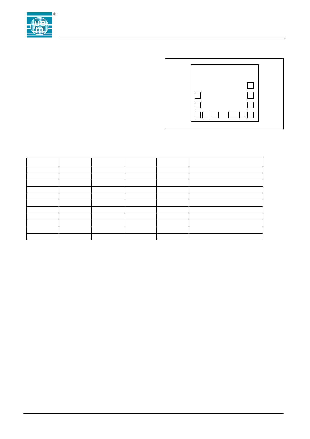
Chip and Packaging Information
Chip size is 57 x 69 mil
Pad Location
EM4022
EM 4 0 2 2
1
2
34 5
6
11
10
9
78
Pad location table with reference on pad 3 center :
Pad N°
X [µm]
Y [µm]
size [µm]
1
0
417
98/98
2
0
234
98/98
3
0
0
98/98
4
125
0
98/98
5
228
0
175/98
6
1037
0
175/98
7
1200
-13
98/98
8
1324
1
98/98
9
1324
196
98/98
10
1324
374
98/98
11
1324
552
Test inputs and outputs must be left open.
98/98
Pad name
XCLK
VDD
M
MTST
COIL1
COIL2
VSSTST
VSS
GAP
SI
TMC
Function
external test clock input
positive supply
connection to antenna
test output
Coil terminal 1
Coil terminal 2
negative test supply output
negative supply
GAP input
Serial test data input (pull down)
Test mode control (pull down)
Fig. 16
Copyright 2002, EM Microelectronic-Marin SA
14
www.emmicroelectronic.com
Share Link: