RF2459 데이터 시트보기 (PDF) - RF Micro Devices
부품명
상세내역
일치하는 목록
RF2459 Datasheet PDF : 8 Pages
| |||
RF2459
Preliminary
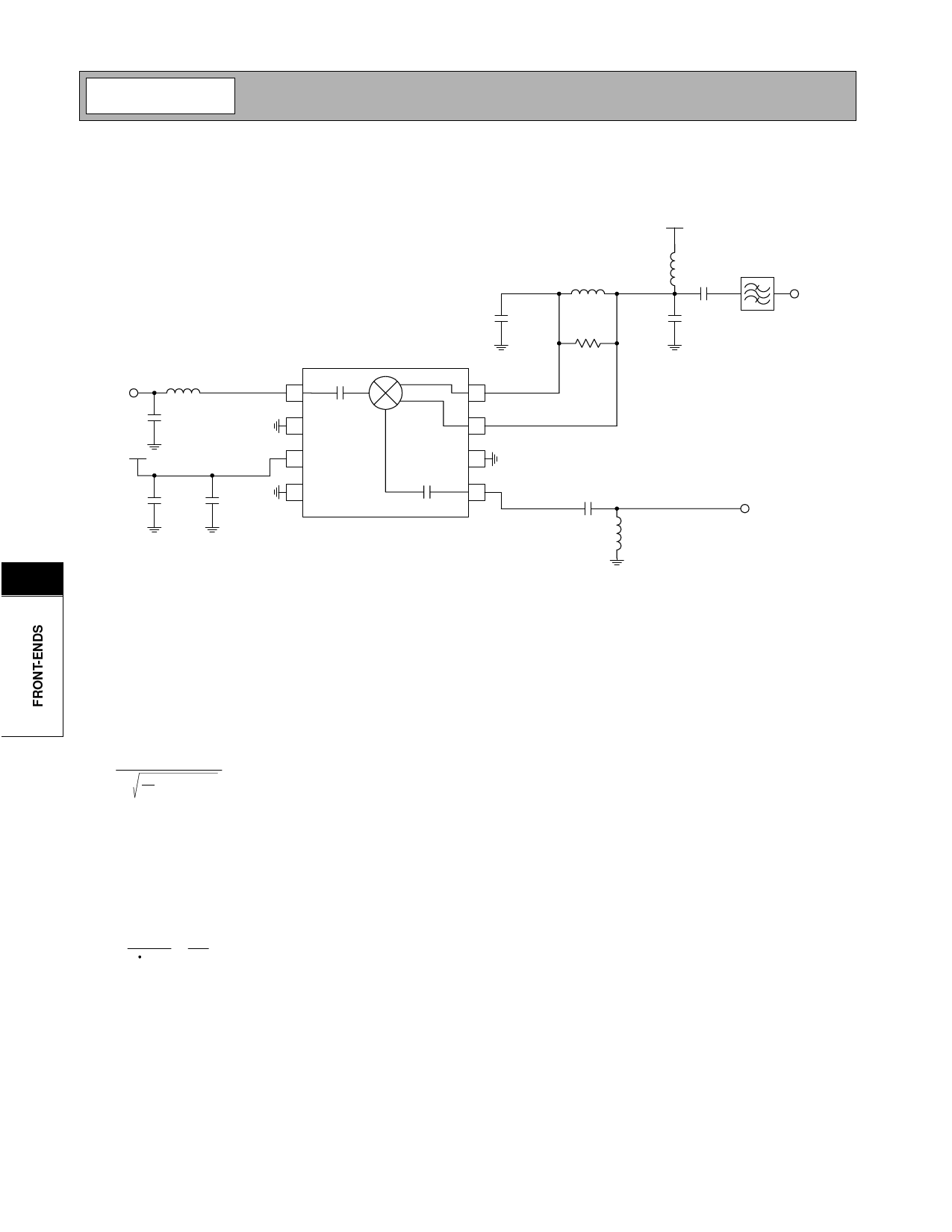
Application Schematic
VCC
L2
IF Filter
L1
C2
IF OUT
C1
C1
R
4.7 nH
LO IN
1
1.5 pF
2
VCC
3
4
100 nF 22 pF
8
7
6
5
1.5 pF
2.2 nH
RF IN
8
Output Interface Network
L1, C1 and R form a current combiner which performs
a differential to single-ended conversion at the IF fre-
quency and sets the output impedance. In most cases,
the resonance frequency is independent of R and can
be set according to the following equation:
fIF =
2π
1
L21(C1 + CEQ)
Where CEQ is the equivalent stray capacitance and
capacitance looking into pins 7 and 8. An average
value to use for CEQ is 2.5pF.
R can then be used to set the output impedance
according to the following equation:
( ) R =
4
1
ROUT
-
1
RP
-1
where ROUT is the desired output impedance and RP is
the parasitic equivalent parallel resistance of L1.
C1 should be chosen as high as possible, while main-
taining an RP of L1 that allows for the desired ROUT.
L2 and C2 serve dual purposes. L2 serves as an out-
put bias choke, and C2 serves as a series DC block.
In addition, L2 and C2 may be chosen to form an
impedance matching network if the input impedance of
the IF filter is not equal to ROUT. Otherwise, L2 is cho-
sen to be large (suggested 8.2nH) and C2 is chosen to
be large (suggested 22nF) if a DC path to ground is
present in the IF filter, or omitted if the filter is DC
blocked.
8-100
Rev A2 010717
Share Link: 