DS2165 데이터 시트보기 (PDF) - Dallas Semiconductor -> Maxim Integrated
부품명
상세내역
일치하는 목록
DS2165 Datasheet PDF : 17 Pages
| |||
DS2165Q
CONTROL REGISTER
The control register establishes idle, algorithm reset, bypass, data format, and channel coding for the
selected channel.
The X-side and Y-side PCM interfaces can be independently disabled (output tri-stated) by IPD. When
IPD is set for both channels, the device enters a low-power standby mode. In this mode, the serial port
must not be operated faster than 39kHz.
ALRST resets the algorithm coefficients for the selected channel to their initial values. ALRST is cleared
by the device when the algorithm reset is complete.
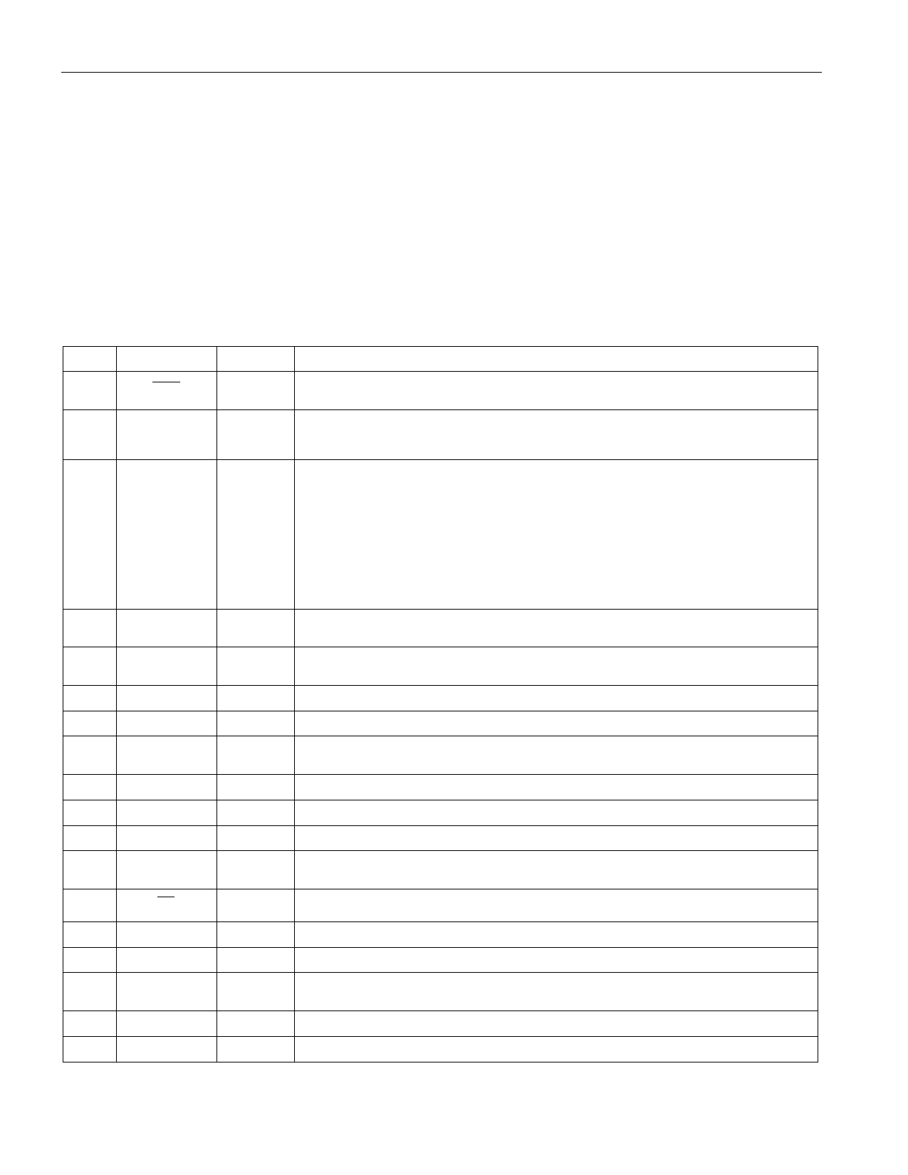
Table 1. PIN DESCRIPTION
PIN SYMBOL
2
RST
3
TM0
4
TM1
6
A0
7
A1
8
A2
9
A3
10
A4
11
A5
12
SPS
13
MCLK
14
VSS
16
XIN
17
CLKX
18
FSX
20
XOUT
21
SCLK
22
SDI
23
CS
24
YOUT
25
FSY
26
CLKY
27
YIN
28
VDD
TYPE
I
FUNCTION
Reset. A high-low-high transition resets the algorithm. The device should be
reset on power-up and when changing to or from the hardware mode.
I
Test Modes 0 and 1. Connect to VSS for normal operation.
I
Address Select. A0 = LSB, A5 = MSB. Must match address/command word
to enable the serial port.
I
Serial Port Select. Connect to VDD to select the serial port; connect to VSS to
select the hardware mode.
I
Master Clock. 10MHz clock for the ADPCM processing engine; may be
asynchronous to SCLK, CLKX, and CLKY.
— Signal Ground. 0V
I
X Data In. Sampled on falling edge of CLKX during selected time slots.
I
X Data Clock. Data clock for the X-side PCM interface; must be
synchronous with FSX.
I
X Frame Sync. 8kHz frame sync for the X-side PCM interface.
O X Data Output. Updated on rising edge of CLKX during selected time slots.
I
Serial Data Clock. Used to write to the serial port registers.
I
Serial Data In. Data for on-board control registers; sampled on the rising
edge of SCLK. LSB sent first.
I
Chip Select. Must be low to write to the serial port.
O Y Data Output. Updated on rising edge of CLKY during selected time slots.
I
Y Frame Sync. 8kHz frame sync for the Y-side PCM interface.
I
Y Data Clock. Data clock for the Y-side PCM interface; must be
synchronous with FSY.
I
Y Data In. Sampled on falling edge of CLKY during selected time slots.
— Positive Supply. 5.0V (3.0V for DS2165QL)
3 of 17
Share Link: 