DM74LS273SJX 데이터 시트보기 (PDF) - Fairchild Semiconductor
부품명
상세내역
일치하는 목록
DM74LS273SJX Datasheet PDF : 6 Pages
| |||
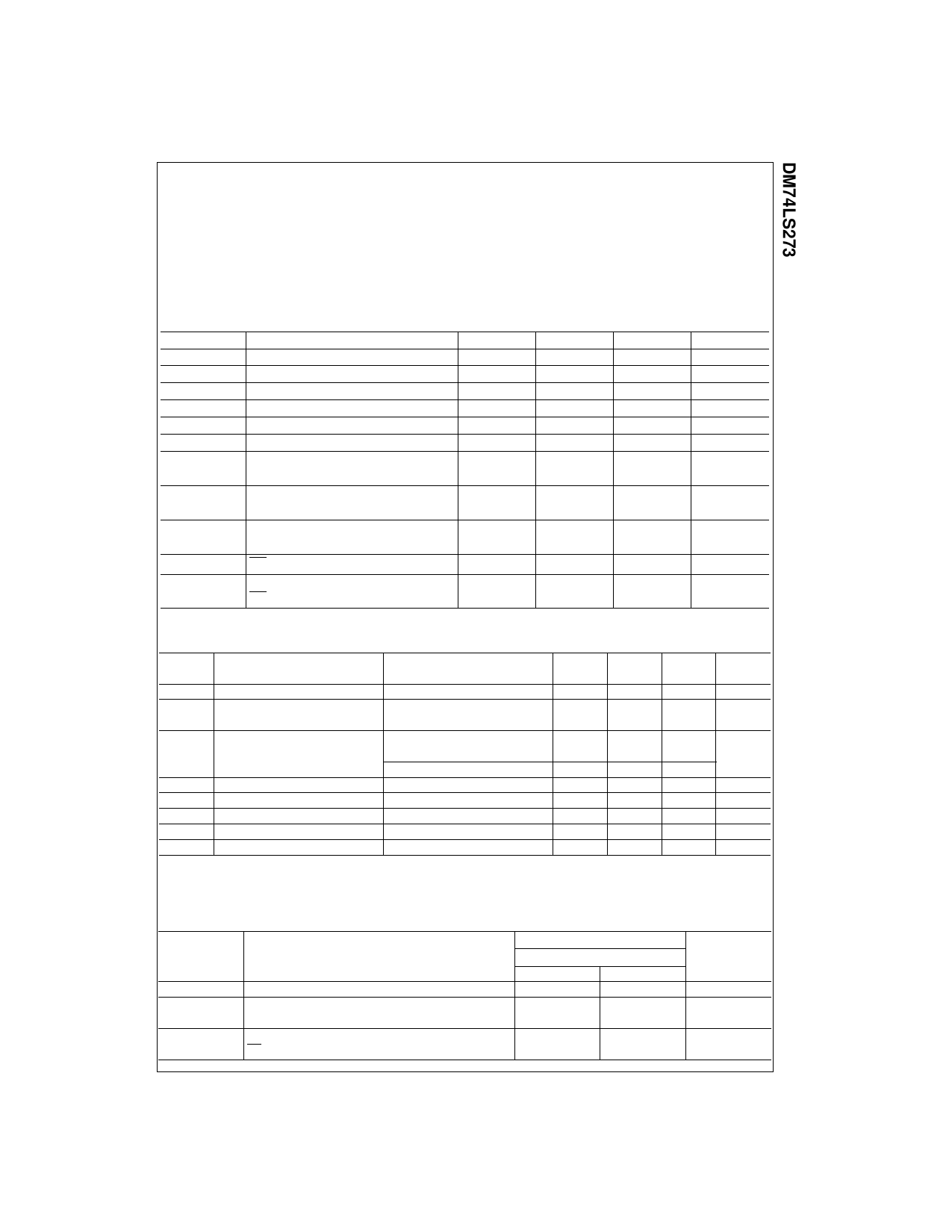
Absolute Maximum Ratings(Note 1)
Supply Voltage
7V
Input Voltage
7V
Operating Free Air Temperature Range 0°C to +70°C
Storage Temperature Range
−65°C to +150°C
Note 1: The “Absolute Maximum Ratings” are those values beyond which
the safety of the device cannot be guaranteed. The device should not be
operated at these limits. The parametric values defined in the Electrical
Characteristics tables are not guaranteed at the absolute maximum ratings.
The “Recommended Operating Conditions” table will define the conditions
for actual device operation.
Recommended Operating Conditions
Symbol
VCC
VIH
VIL
IOH
IOL
TA
tS(H)
tS(L)
tH(H)
tH(L)
tW(H)
tW(L)
tW(L)
tREC
Parameter
Supply Voltage
HIGH Level Input Voltage
LOW Level Input Voltage
HIGH Level Output Current
LOW Level Output Current
Free Air Operating Temperature
Setup Time HIGH or LOW
Dn to CP
Hold Time HIGH or LOW
Dn to CP
CP Pulse Width HIGH or LOW
MR Pulse Width LOW
Recovery Time
MR to CP
Min
Nom
Max
Units
4.75
5
5.25
V
2
V
0.8
V
−0.4
mA
8
mA
0
70
°C
15
ns
15
5
ns
5
20
ns
20
20
ns
15
ns
Electrical Characteristics
Over recommended operating free air temperature range (unless otherwise noted)
Symbol
Parameter
Conditions
Min
VI
Input Clamp Voltage
VCC = Min, II = −18 mA
VOH
HIGH Level
Output Voltage
VCC = Min, IOH = Max,
2.7
VIL = Max
VOL
LOW Level
VCC = Min, IOL = Max,
Output Voltage
VIH = Min
IOL = 4 mA, VCC = Min
II
Input Current @ Max Input Voltage
VCC = Max, VI = 7V
IIH
HIGH Level Input Current
VCC = Max, VI = 2.7V
IIL
LOW Level Input Current
VCC = Max, VI = 0.4V
IOS
Short Circuit Output Current
VCC = Max (Note 3)
−20
ICC
Supply Current
VCC = Max
Note 2: All typicals are at VCC = 5V, TA = 25°C.
Note 3: Not more than one output should be shorted at a time, and the duration should not exceed one second.
Typ
(Note 2)
3.4
0.35
0.25
Switching Characteristics
VCC = +5.0V, TA =+25°C
Symbol
Parameter
fMAX
tPLH
tPHL
tPLH
Maximum Clock Frequency
Propagation Delay
CP to Qn
Propagation Delay
MR to Qn
CL = 15 pF
RL = 2 kΩ
Min
Max
30
24
24
27
Max
−1.5
0.5
0.4
0.1
20
−0.4
−100
27
Units
V
V
V
mA
µA
mA
mA
mA
Units
MHz
ns
ns
3
www.fairchildsemi.com
Share Link: 