DG9451 데이터 시트보기 (PDF) - Vishay Semiconductors
부품명
상세내역
일치하는 목록
DG9451 Datasheet PDF : 13 Pages
| |||
www.vishay.com
DG9451, DG9453
Vishay Siliconix
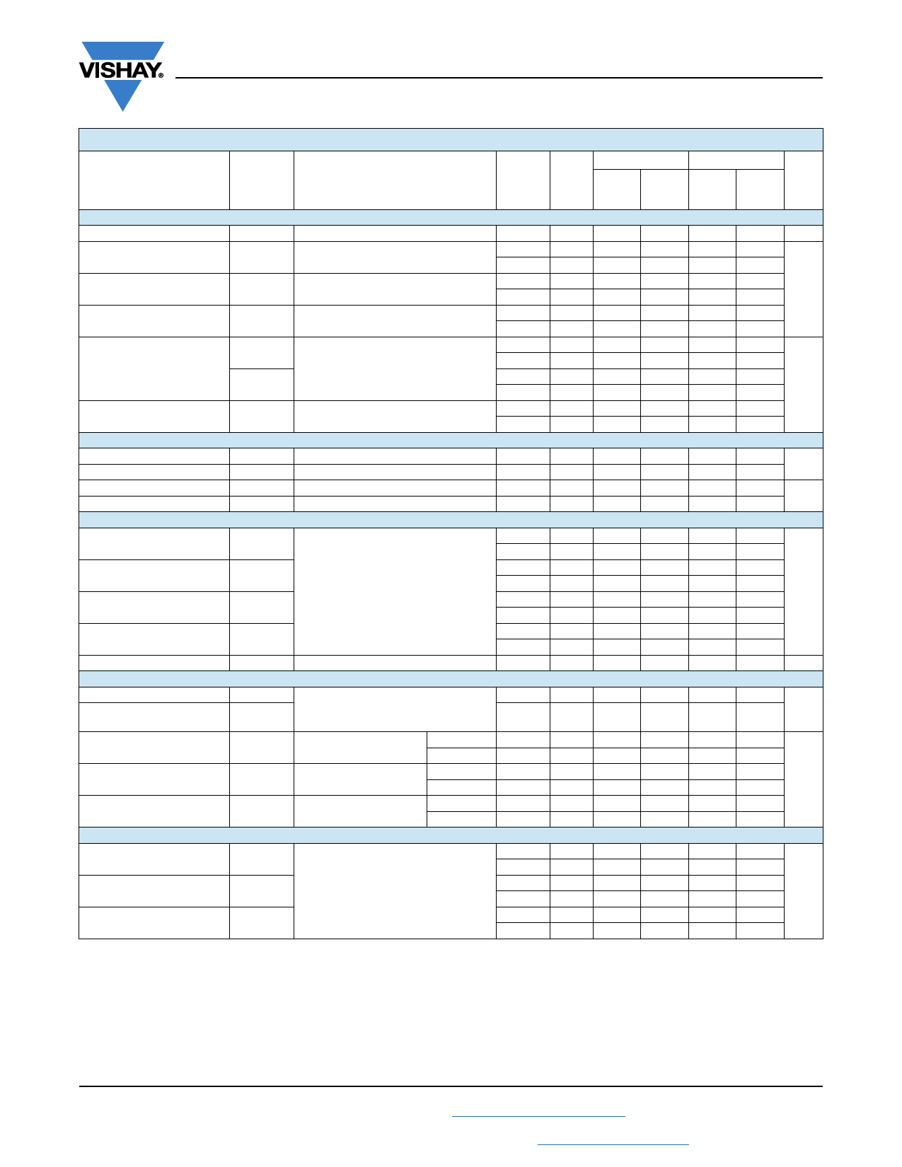
SPECIFICATIONS FOR UNIPOLAR SUPPLIES
PARAMETER
SYMBOL
TEST CONDITIONS
UNLESS OTHERWISE SPECIFIED
VCC = +12 V, VEE = 0 V
V = 1.6 V, 0.5 V a
-40 °C to +125 °C -40 °C to +85 °C
TEMP. b TYP. c
MAX. d MIN. d MIN. d
MAX.
UNIT
D
Analog Switch
Analog Signal Range e
VANALOG
Full
-
0
12
0
12
V
On-Resistance
Room 68
-
105
-
105
RON
IS = 1 mA, VD = 0.7 V, 6 V, 11.3 V
Full
-
-
143
-
137
On-Resistance Match
ΔRON
IS = 1 mA, VD = +0.7 V
Room 4
Full
-
-
7
-
-
10
-
7
8
Ω
Room 32
-
45
-
45
On-Resistance Flatness RFLATNESS
IS = 1 mA, VD = 0.7 V, +11.3 V
Full
-
-
49
-
47
Switch Off
Leakage Current
IS(off)
ID(off)
V+ = +12 V, V- = 0 V
VD = 1 V/11 V, VS = 11 V/1 V
Room ± 0.02 -1
1
-1
Full
-
-50
50
-5
Room ± 0.02 -1
1
-1
Full
-
-50
50
-5
1
5
1
5
nA
Channel On
Leakage Current
ID(on)
V+ = +12 V, V- = 0 V
VD = VS = 1 V/11 V
Room ± 0.02 -1
1
-1
1
Full
-
-50
50
-5
5
Digital Control
VIN(A, B, C and ENABLE) Low
VIL
VIN(A, B, C and ENABLE) High
VIH
Full
-
-
0.5
-
0.5
Full
-
1.6
-
1.6
-
V
Input Current, VIN Low
Input Current, VIN High
IL
VIN(A, B, C and ENABLE) under test = 0.5 V Full
0.01
-1
1
-1
1
μA
IH
VIN(A, B, C and ENABLE) under test = 1.6 V Full
0.01
-1
1
-1
1
Dynamic Characteristics
Transition Time
tTRANS
Room 55
-
135
-
135
Full
-
-
166
-
155
Enable Turn-On Time
tON
Enable Turn-Off Time
tOFF
RL = 300 Ω, CL = 35 pF
see figure 1, 2, 3
Room 106
-
185
-
185
Full
-
Room 65
-
-
219
130
-
-
205
130
ns
Full
-
-
144
-
137
Break-Before-Make
Time Delay
tD
Room 30
-
-
-
-
Full
-
-
12
-
12
Charge Injection e
Q
Vg = 0 V, Rg = 0 Ω, CL = 1 nF
Room 0.79
-
-
-
-
pC
Dynamic Characteristics
Off Isolation e
Channel-to-Channel
Crosstalk e
OIRR
XTALK
RL = 50 Ω, CL = 15 pF
f = 100 kHz
Room < -90 -
-
-
-
dB
Room < -90 -
-
-
-
Source Off Capacitance e CS(off)
f = 1 MHz
DG9451 Room 1
-
-
-
-
DG9453 Room 1
-
-
-
-
Drain Off Capacitance e
CD(off)
f = 1 MHz
DG9451 Room 9
-
-
-
-
DG9453 Room 3
-
-
-
-
pF
Channel On Capacitance e CD(on)
f = 1 MHz
DG9451 Room 15
-
-
-
-
DG9453 Room 8
-
-
-
-
Power Supplies
Power Supply Current
I+
Room 0.05
-
1
-
1
Full
-
-
10
-
10
Negative Supply Current
I-
Room -0.05 -1
-
-1
-
VIN(A, B, C and ENABLE) = 0 V or 12 V
Full
-
-10
-
-10
μA
-
Ground Current
IGND
Room -0.05 -1
-
-1
-
Full
-
-10
-
-10
-
Notes
a. VIN = input voltage to perform proper function.
b. Room -25 °C, Full = as determined by the operating temperature suffix.
c. Typical values are for DESIGN AID ONLY, not guaranteed nor subject to production testing.
d. The algebraic convention whereby the most negative value is a minimum and the most positive a maximum, is used in this data sheet.
e. Guaranteed by design, not subject to production test.
Stresses beyond those listed under “Absolute Maximum Ratings” may cause permanent damage to the device. These are stress ratings only, and functional operation
of the device at these or any other conditions beyond those indicated in the operational sections of the specifications is not implied. Exposure to absolute maximum
rating conditions for extended periods may affect device reliability.
S14-2340-Rev. C, 08-Dec-14
5
Document Number: 65020
For technical questions, contact: powerictechsupport@vishay.com
THIS DOCUMENT IS SUBJECT TO CHANGE WITHOUT NOTICE. THE PRODUCTS DESCRIBED HEREIN AND THIS DOCUMENT
ARE SUBJECT TO SPECIFIC DISCLAIMERS, SET FORTH AT www.vishay.com/doc?91000
Share Link: 