DG506AAK 데이터 시트보기 (PDF) - Vishay Semiconductors
부품명
상세내역
일치하는 목록
DG506AAK Datasheet PDF : 8 Pages
| |||
DG506A_MIL/507A_MIL
Vishay Siliconix
APPLICATION HINTSa
V+
Positive Supply
Voltage
(V)
V–
Negative Supply
Voltage
(V)
VIN
Logic Input Voltage
VINH(min)/VINL(max)
(V)
VS or VD
Analog Voltage
Range
(V)
15b
–15
12
–12
10
–10
8c
–8
2.4/0.8
2.4/0.8
2.2/0.6
2.0/0.5
–15 to 15
–12 to 12
–10 to 10
–8 to 8
Notes:
a. Application Hints are for DESIGN AID ONLY, not guaranteed and not subject to production testing.
b. Electrical Parameter Chart based on V+ = 15 V, V– = –15 V.
c. Operation below "8 V is not recommended due to shift in VINL(MAX).
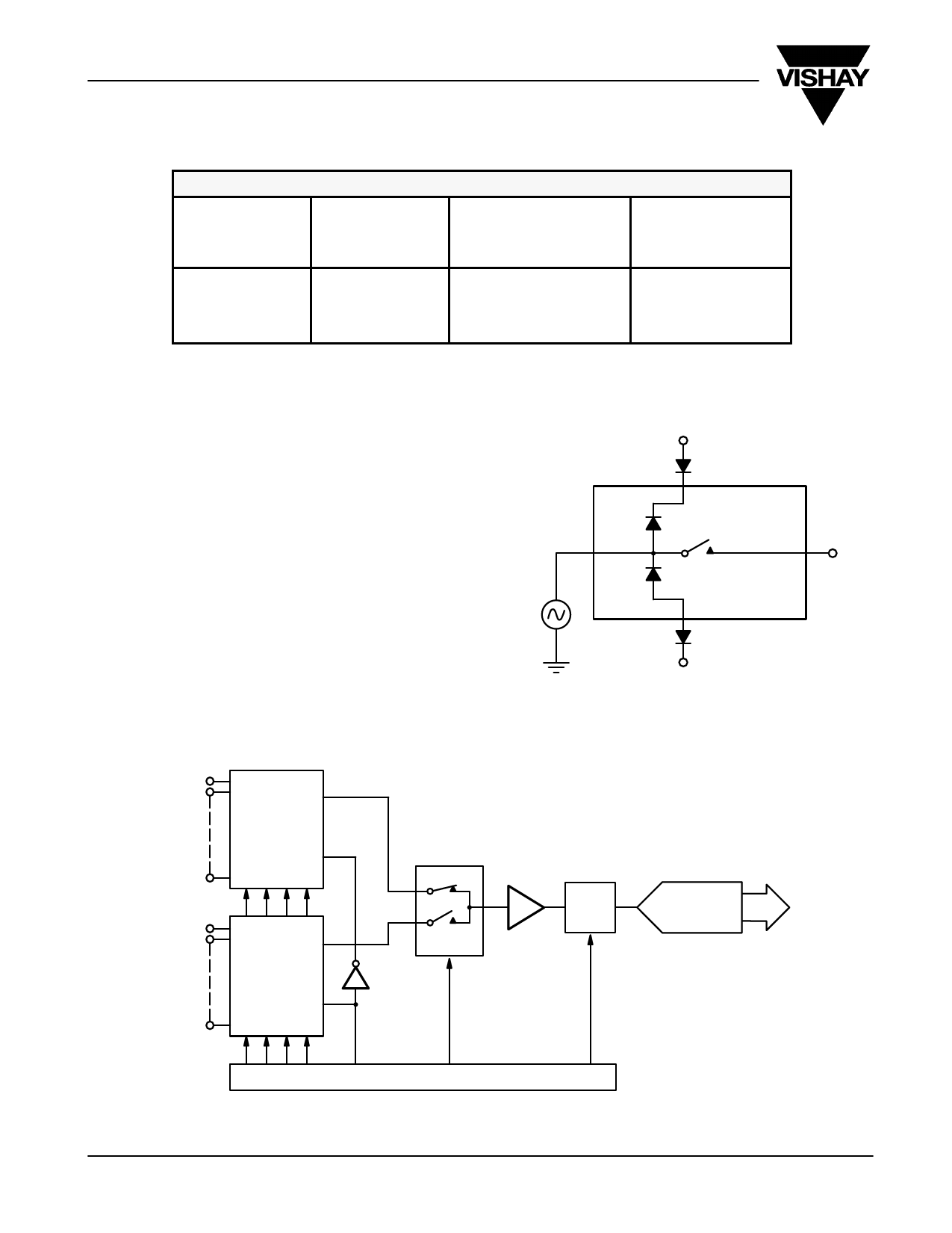
Overvoltage Protection
A very convenient form of overvoltage protection consists of
adding two small signal diodes (1N4148, 1N914 type) in series
with the supply pins (see Figure 5). This arrangement
effectively blocks the flow of reverse currents. It also floats the
supply pin above or below the normal V+ or V– value. In this
case the overvoltage signal actually becomes the power
supply of the IC. From the point of view of the chip, nothing has
changed, as long as the difference between VS and the V– rail
doesn’t exceed +44 V. The addition of these diodes will reduce
the analog signal range to 1 V below V+ and 1 V above V–, but
it preserves the low channel resistance and low leakage
characteristics.
V+ v Vg vV–
SX
Vg
+V
1N4148
+V
Internal
Junction
Internal
Junction
DG506A_MIL
DG507A_MIL
–V
1N4148
–V
FIGURE 5. Overvoltage Protection Using Blocking Diodes
Channel 1
Channel 2
Channel 16
D
DG506A_MIL
#1
EN
A0 A1 A2 A3
Channel 17
Channel 18
Channel 32
D
DG506A_MIL
#2
EN
A0 A1 A2 A3
A
S/H
DG419
Controller
www.vishay.com S FaxBack 408-970-5600
5-8
FIGURE 6. A 32-Channel Data Acquisition System
A/D
Data
Bus
Document Number: 70066
S-00405—Rev. D, 21-Feb-00
Share Link: 