DG528 데이터 시트보기 (PDF) - Intersil
부품명
상세내역
일치하는 목록
DG528 Datasheet PDF : 16 Pages
| |||
DG526, DG527, DG528, DG529
Minimum Input Timing Requirements Over Full Temperature Range
PARAMETER
MEASURED TERMINAL
MIN
UNITS
WRITE Pulse Width, tWW
WR, See Figure 1
300
ns
A, EN Data Valid After WRITE (Stabilization Time), tDW A0, A1, (A2), EN, WR; See Figure 1
180
ns
A, EN Data Valid After WRITE (Hold Time), tWD
A0, A1, (A2), EN, WR; See Figure 1
30
ns
RESET Pulse Width, tRS
RS, (Note 6), VS = 5V, See Figure 2
500
ns
NOTES:
1. Signals on VS, VD or VIN exceeding V+ or V- will be clamped by internal diodes. Limit diode forward current to maximum current ratings.
2. Typical values are for design aid only, not guaranteed and not subject to production testing.
3. The algebraic convention whereby the most negative value is a minimum, and most positive value is a maximum, is used in this datasheet.
4.
OFF Isolation
=
20--V----S--- , where
VD
VS =
input
to OFF switch, and
VD = output
due to
VS .
5. ID(ON) is leakage from driver into “ON” switch.
6. Period of Reset (RS) pulse must be at least 50µs during or after power ON.
7. Parameter not tested. Parameter guaranteed by design or characterization.
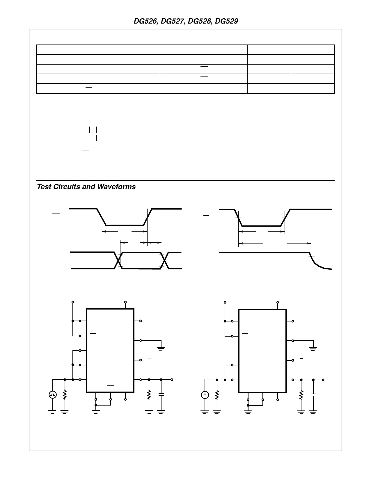
Test Circuits and Waveforms
3V
WR
0
3V
A0, A1, (A2)
EN
0
1.5V
tWW
tDW
2.0V
tWD
0.8V
FIGURE 1. WR TIMING WAVEFORMS
3V
RS
0
VO
SWITCH
OUTPUT
0V
1.5V
tRS
tOFF(RS)
0.8VO
FIGURE 2. RS TIMING WAVEFORMS
+2.4V
LOGIC
INPUT
50Ω
+15V
V+
EN DG528† S1
±10V
RS
S2 THRU S7
A0
S8
+10V
A1
SWITCH
OUTPUT
A2
D
VD
GND WR V-
1MΩ
35pF
-15V
+2.4V
LOGIC
INPUT
50Ω
+15V
V+
EN
S1B
DG529†
±10V
RS
S2A THRU S4A ,
DA
S2B, AND S3B
S4B
+10V
A0
SWITCH
A1
DB
OUTPUT
VDB
GND WR V-
1MΩ
35pF
-15V
FIGURE 3A. tTRANSITION SWITCHING TIME TEST CIRCUIT
† Similar connections for DG526
FIGURE 3B. tTRANSITION SWITCHING TIME TEST CIRCUIT
† Similar connections for DG527
12-8
Share Link: 