HD66130T 데이터 시트보기 (PDF) - Hitachi -> Renesas Electronics
부품명
상세내역
일치하는 목록
HD66130T
Hitachi -> Renesas Electronics

HD66130T Datasheet PDF : 16 Pages
| |||
HD66130T
1. Liquid crystal drive circuit
Selects and outputs the liquid crystal drive level V0, VM, or V1 by DISP and a combination of data for
latch circuit 2 and signal M.
2. Level shifter
Converts logic signals to liquid crystal drive signals.
3. Latch circuit 2
320-bit latch circuit, which latches the data of latch circuits 1 at the fall of CL1 and outputs the data to
the level shifter.
4. Latch circuit 1
4/8-bit parallel data latch circuit, which latches display data D0 to D7 according to signals transmitted
from the shift register.
5. Shift register
80-bit shift register, which generates data-capture signals for latch circuits 1 at the fall of CL2.
6. Data rearrangement circuit
Inverts the order of data output crosswise.
7. Timing generator circuit
The timing generator circuit generates data latch pulses for latch circuit2 and changes pulse the LCD
drive outputs to AC.
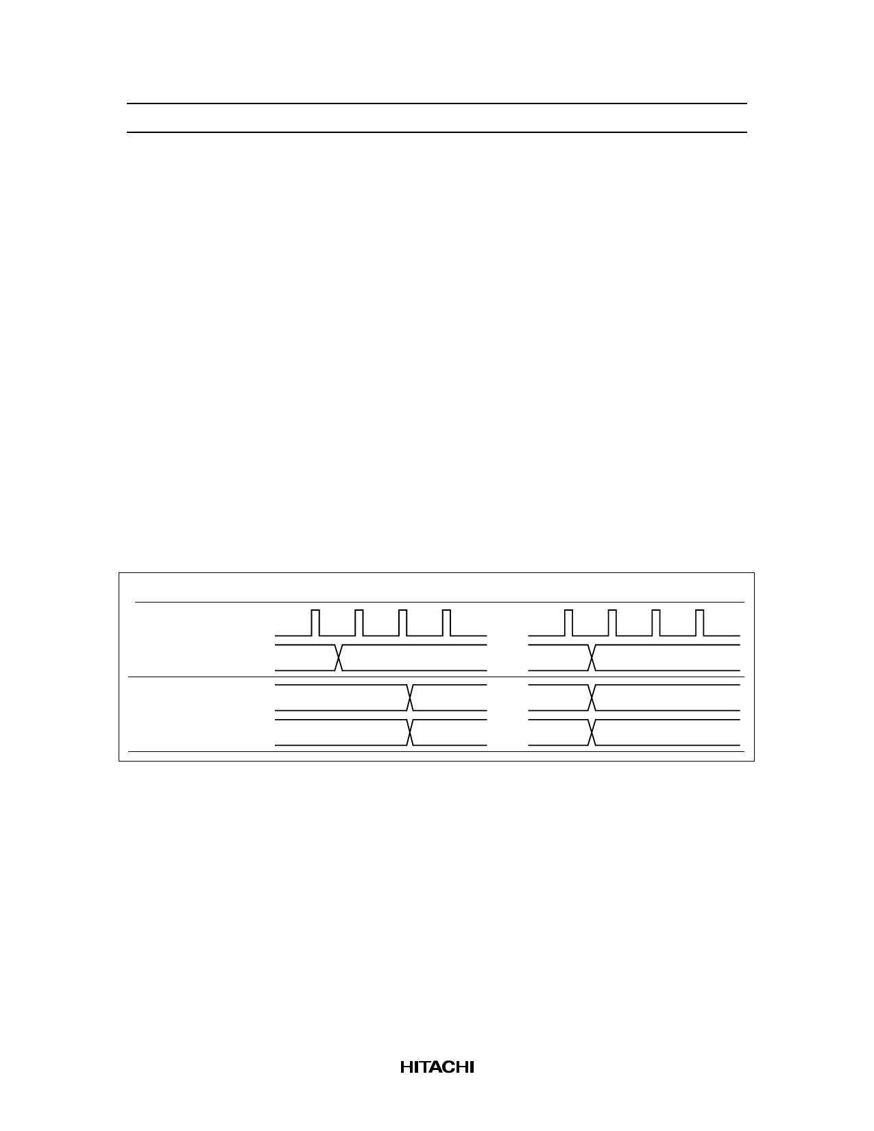
HIFAS Family timing Comparision
Input
signal
HD66130/131/134/135
CL1
M
Output
signal
Segment
Common
HD66132/133
3
Share Link: