CY7C140 데이터 시트보기 (PDF) - Cypress Semiconductor
부품명
상세내역
일치하는 목록
CY7C140 Datasheet PDF : 19 Pages
| |||
CY7C130/CY7C131
CY7C140/CY7C141
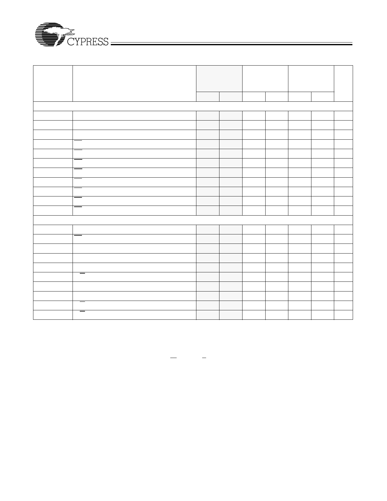
Switching Characteristics Over the Operating Range[6, 11]
7C131-15[3]
7C141-15
7C130-25[3]
7C131-25
7C140-25
7C141-25
7C130-30
7C131-30
7C140-30
7C141-30
Parameter
Description
Min. Max. Min. Max. Min. Max. Unit
READ CYCLE
tRC
Read Cycle Time
tAA
Address to Data Valid[12]
tOHA
Data Hold from Address Change
tACE
CE LOW to Data Valid[12]
tDOE
OE LOW to Data Valid[12]
tLZOE
OE LOW to Low Z[9, 13, 14]
tHZOE
OE HIGH to High Z[9, 13, 14]
tLZCE
CE LOW to Low Z[9, 13, 14]
tHZCE
CE HIGH to High Z[9, 13, 14]
tPU
CE LOW to Power-Up[9]
tPD
CE HIGH to Power-Down[9]
WRITE CYCLE[15]
15
25
30
ns
15
25
30 ns
0
0
0
ns
15
25
30 ns
10
15
20 ns
3
3
3
ns
10
15
15 ns
3
5
5
ns
10
15
15 ns
0
0
0
ns
15
25
25 ns
tWC
Write Cycle Time
15
25
30
ns
tSCE
CE LOW to Write End
12
20
25
ns
tAW
Address Set-Up to Write End
12
20
25
ns
tHA
Address Hold from Write End
2
2
2
ns
tSA
Address Set-Up to Write Start
0
0
0
ns
tPWE
R/W Pulse Width
12
15
25
ns
tSD
Data Set-Up to Write End
10
15
15
ns
tHD
tHZWE
tLZWE
Data Hold from Write End
R/W LOW to High Z[14]
R/W HIGH to Low Z[14]
0
0
0
ns
10
15
15 ns
0
0
0
ns
Shaded areas contain preliminary information.
Note:
11. Test conditions assume signal transition times of 5 ns or less, timing reference levels of 1.5V, input pulse levels of 0 to 3.0V and output loading of the specified
IOL/IOH, and 30-pF load capacitance.
12. AC Test Conditions use VOH = 1.6V and VOL = 1.4V.
13. At any given temperature and voltage condition for any given device, tHZCE is less than tLZCE and tHZOE is less than tLZOE.
14. tLZCE, tLZWE, tHZOE, tLZOE, tHZCE and tHZWE are tested with CL = 5pF as in part (b) of AC Test Loads. Transition is measured ±500 mV from steady state voltage.
15. The internal write time of the memory is defined by the overlap of CS LOW and R/W LOW. Both signals must be low to initiate a write and either signal can
terminate a write by going high. The data input set-up and hold timing should be referenced to the rising edge of the signal that terminates the write.
Document #: 38-06002 Rev. *D
Page 5 of 19
Share Link: 