CY7C026A-12AC 데이터 시트보기 (PDF) - Cypress Semiconductor
부품명
상세내역
일치하는 목록
CY7C026A-12AC Datasheet PDF : 18 Pages
| |||
CY7C026A
CY7C036A
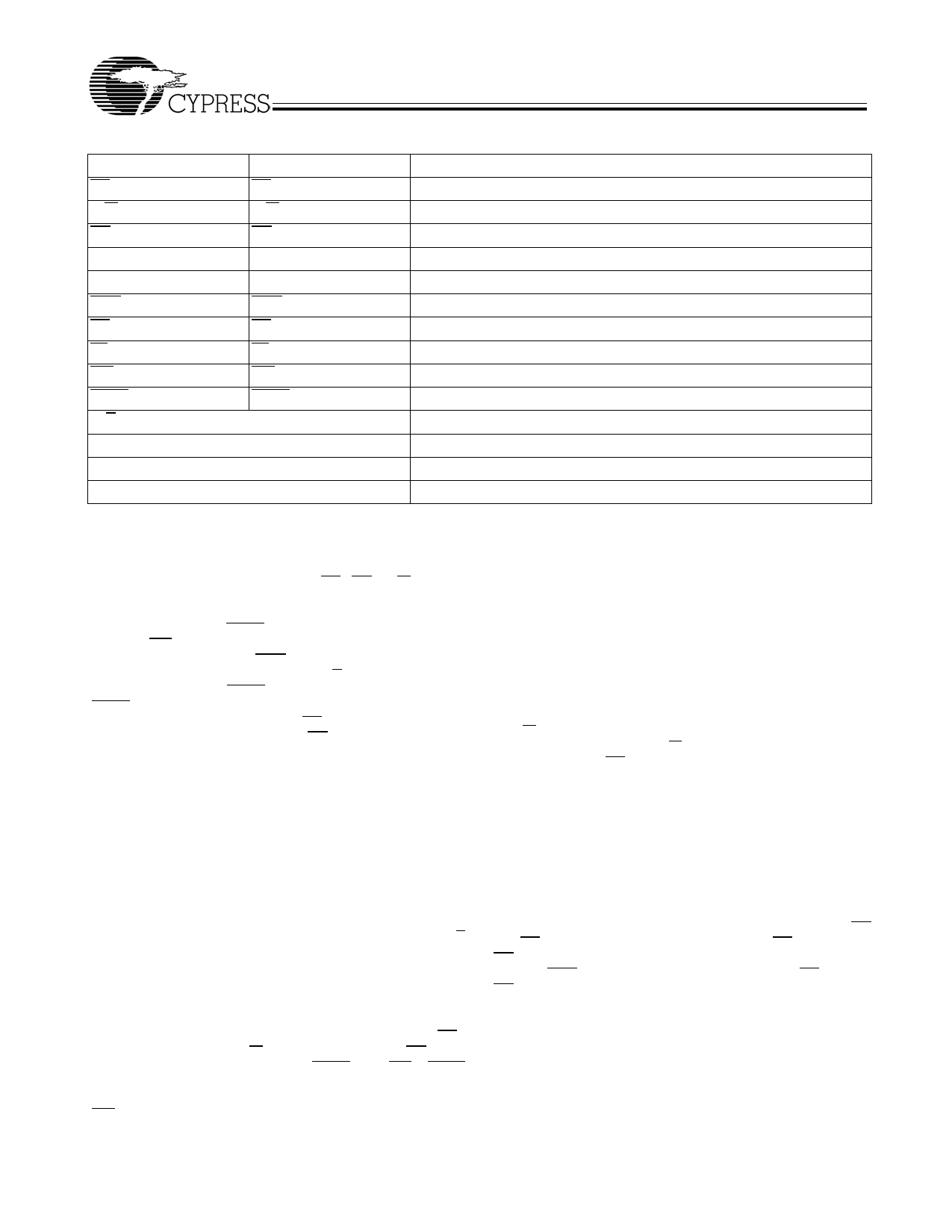
Pin Definitions
Left Port
CEL
R/WL
OEL
A0L–A13L
I/O0L–I/O17L
SEML
UBL
LBL
INTL
BUSYL
M/S
VCC
GND
NC
Right Port
CER
R/WR
OER
A0R–A13R
I/O0R–I/O17R
SEMR
UBR
LBR
INTR
BUSYR
Description
Chip Enable
Read/Write Enable
Output Enable
Address
Data Bus Input/Output
Semaphore Enable
Upper Byte Select (I/O8–I/O15 for x16 devices; I/O9–I/O17 for x18 devices)
Lower Byte Select (I/O0–I/O7 for x16 devices; I/O0–I/O8 for x18 devices)
Interrupt Flag
Busy Flag
Master or Slave Select
Power
Ground
No Connect
Architecture
The CY7C026A and CY7C036A consist of an array of 16K
words of 16 and 18 bits each of dual-port RAM cells, I/O and
address lines, and control signals (CE, OE, R/W). These
control pins permit independent access for reads or writes to
any location in memory. To handle simultaneous writes/reads
to the same location, a BUSY pin is provided on each port. Two
Interrupt (INT) pins can be utilized for port-to-port communi-
cation. Two Semaphore (SEM) control pins are used for
allocating shared resources. With the M/S pin, the devices can
function as a master (BUSY pins are outputs) or as a slave
(BUSY pins are inputs). The devices also have an automatic
power-down feature controlled by CE. Each port is provided
with its own Output Enable control (OE), which allows data to
be read from the device.
Functional Description
The CY7C026A and CY7C036A are low-power CMOS 16K x
16/18 dual-port static RAMs. Various arbitration schemes are
included on the devices to handle situations when multiple
processors access the same piece of data. Two ports are
provided, permitting independent, asynchronous access for
reads and writes to any location in memory. The devices can
be utilized as standalone 16/18-bit dual-port static RAMs or
multiple devices can be combined in order to function as a
32/36-bit or wider master/slave dual-port static RAM. An M/S
pin is provided for implementing 32/36-bit or wider memory
applications without the need for separate master and slave
devices or additional discrete logic. Application areas include
interprocessor/multiprocessor designs, communications
status buffering, and dual-port video/graphics memory.
Each port has independent control pins: Chip Enable (CE),
Read or Write Enable (R/W), and Output Enable (OE). Two
flags are provided on each port (BUSY and INT). BUSY
signals that the port is trying to access the same location
currently being accessed by the other port. The Interrupt flag
(INT) permits communication between ports or systems by
means of a mail box. The semaphores are used to pass a flag,
or token, from one port to the other to indicate that a shared
resource is in use. The semaphore logic is comprised of eight
shared latches. Only one side can control the latch
(semaphore) at any time. Control of a semaphore indicates
that a shared resource is in use. An automatic power-down
feature is controlled independently on each port by the chip
enable pin.
The CY7C026A and CY7C036A are available in 100-pin Thin
Quad Plastic Flatpack (TQFP) packages.
Write Operation
Data must be set up for a duration of tSD before the rising edge
of R/W in order to guarantee a valid write. A write operation is
controlled by either the R/W pin (see Write Cycle No. 1
waveform) or the CE pin (see Write Cycle No. 2 waveform).
Required inputs for non-contention operations are summa-
rized in Table 1.
If a location is being written to by one port and the opposite
port attempts to read that location, a port-to-port flowthrough
delay must occur before the data is read on the output;
otherwise the data read is not deterministic. Data will be valid
on the port tDDD after the data is presented on the other port.
Read Operation
When reading the device, the user must assert both the OE
and CE pins. Data will be available tACE after CE or tDOE after
OE is asserted. If the user wishes to access a semaphore flag,
then the SEM pin must be asserted instead of the CE pin, and
OE must also be asserted.
Interrupts
The upper two memory locations may be used for message
passing. The highest memory location (3FFF) is the mailbox
for the right port and the second-highest memory location
(3FFE) is the mailbox for the left port. When one port writes to
the other port’s mailbox, an interrupt is generated to the owner.
Document #: 38-06046 Rev. *C
Page 4 of 18
Share Link: 