CY22313 데이터 시트보기 (PDF) - Cypress Semiconductor
부품명
상세내역
일치하는 목록
CY22313 Datasheet PDF : 9 Pages
| |||
CY22313
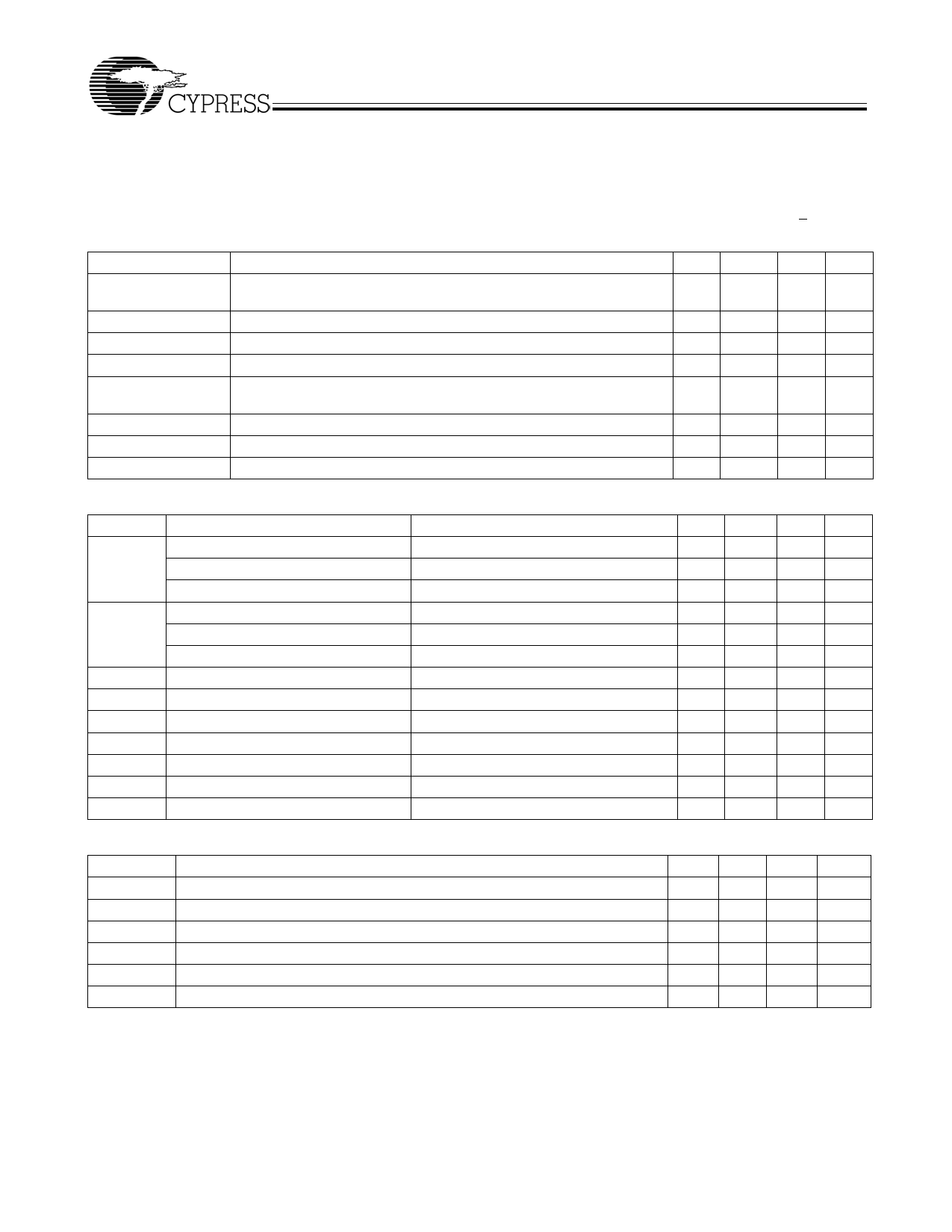
Absolute Maximum Conditions
(Above which the useful life may be impaired. For user guide-
lines; not tested.)
Supply Voltage ............................................... –0.5V to +4.0V
Recommended Operating Conditions[1]
DC Input Voltage ..............................–0.5V to + (VDD + 0.5V)
Storage Temperature .................................. –65°C to +125°C
Static Discharge Voltage
(per MIL-STD-883, Method 3015) ............................... 2000V
Latch-up (per JEDEC 17) .................................... > ±200 mA
Parameter
VDDRP, VDDVPA,
VDDVP, VDDR
VDD54 (2.5V)
VDD54 (1.675V)
VDDL
tPU
TA
CLOAD_54MOUT
fREF
Description
Supply Voltage for PLL’s, Crystal Oscillator, and 3.45V Outputs
Supply Voltage for 2.5V Outputs
Supply Voltage for 1.675V Outputs
Supply Voltage for 1.8V Outputs
Power-up time for all VDDS to reach minimum specified voltage
(power ramps must be monotonic)
Operating Temperature, Ambient
Max. Load Capacitance, CMOS Output
External Reference Crystal
Min. Typ Max. Unit
3.15 3.45 3.6 V
2.25 2.5 2.75 V
1.6 1.675 1.75 V
1.6 1.8 2.0 V
0.05
500 ms
0
+85 °C
15 pF
18.432
MHz
Electrical Specifications
Parameter
Description
Conditions
IOH[2]
IOL[2]
CXTAL
CLOAD_IN
Output High Current, 2.5V outputs[3] VOH = VDD – 0.5, VDD = 2.5V
Output High Current, 1.8V outputs[3] VOH = VDD – 0.5, VDD = 1.8V
Output High Current, 1.675V outputs[3] VOH = VDD – 0.5, VDD = 1.675V
Output Low Current, 2.5V outputs[3] VOL = 0.5V, VDD = 2.5V
Output Low Current, 1.8V outputs[3] VOL = 0.5V, VDD = 1.8V
Output Low Current, 1.675V outputs[3] VOL = 0.5V, VDD = 1.675V
Crystal Load Capacitance[3]
Total effective load of internal load caps
Input Pin Capacitance[3]
Except crystal pins
VIH
HIGH-Level Input Voltage
CMOS levels,% of VDDRP/VDDVPA/VDDVP
VIL
LOW-Level Input Voltage
CMOS levels,% of VDDRP/VDDVPA/VDDVP
RI_FS
FS Input Resistor
Pull-down resistor on FS
RI_S
S Input Resistor
Pull-up resistor on S
IDD
Total Power Supply Current
Sum of all supply currents
Min.
8
6
5
8
6
5
70%
60
10
Typ.
16
12
10
16
12
10
11[4]
7
150
Max.
30%
225
100
125
Unit
mA
mA
mA
mA
mA
mA
pF
pF
VDD
VDD
kΩ
kΩ
mA
Direct Rambus Electrical Specifications[3]
Parameter
Description
Min. Typ. Max. Unit
VCM
VX
VCOS
Differential output common-mode voltage
Differential output crossing-point voltage[5]
Output Voltage swing (p-p single-ended)[6]
1.35
1.75 V
1.25
1.85 V
0.4
0.7
V
VCOH
Output high voltage
2.1
V
VCOL
rOUT
Output low voltage
Output dynamic resistance (at pins)[7]
1.0
V
12
50
Ω
Notes:
1. Unless otherwise noted, Electrical and Switching Characteristics are guaranteed across these operating conditions.
2. LCLK and 54MOUT outputs only.
3. Guaranteed by design, not 100% tested.
4. Identical Crystal Load Capacitance as CY2212ZC-2. Use the same crystal and XIN / XOUT board layout as implemented with the original crystal-driven
CY2212ZC-2.
5. Differential output crossing point voltages shown in Figure 1.
6. VCOS = VOH – VOL.
7. rOUT = ∆ VO/ ∆ IO. This is defined at the output pins, not at the measurement point of Figure 9.
Document #: 38-07434 Rev. *E
Page 3 of 9
Share Link: 