CS8135 데이터 시트보기 (PDF) - Cherry semiconductor
부품명
상세내역
일치하는 목록
CS8135 Datasheet PDF : 8 Pages
| |||
Circuit Description: continued
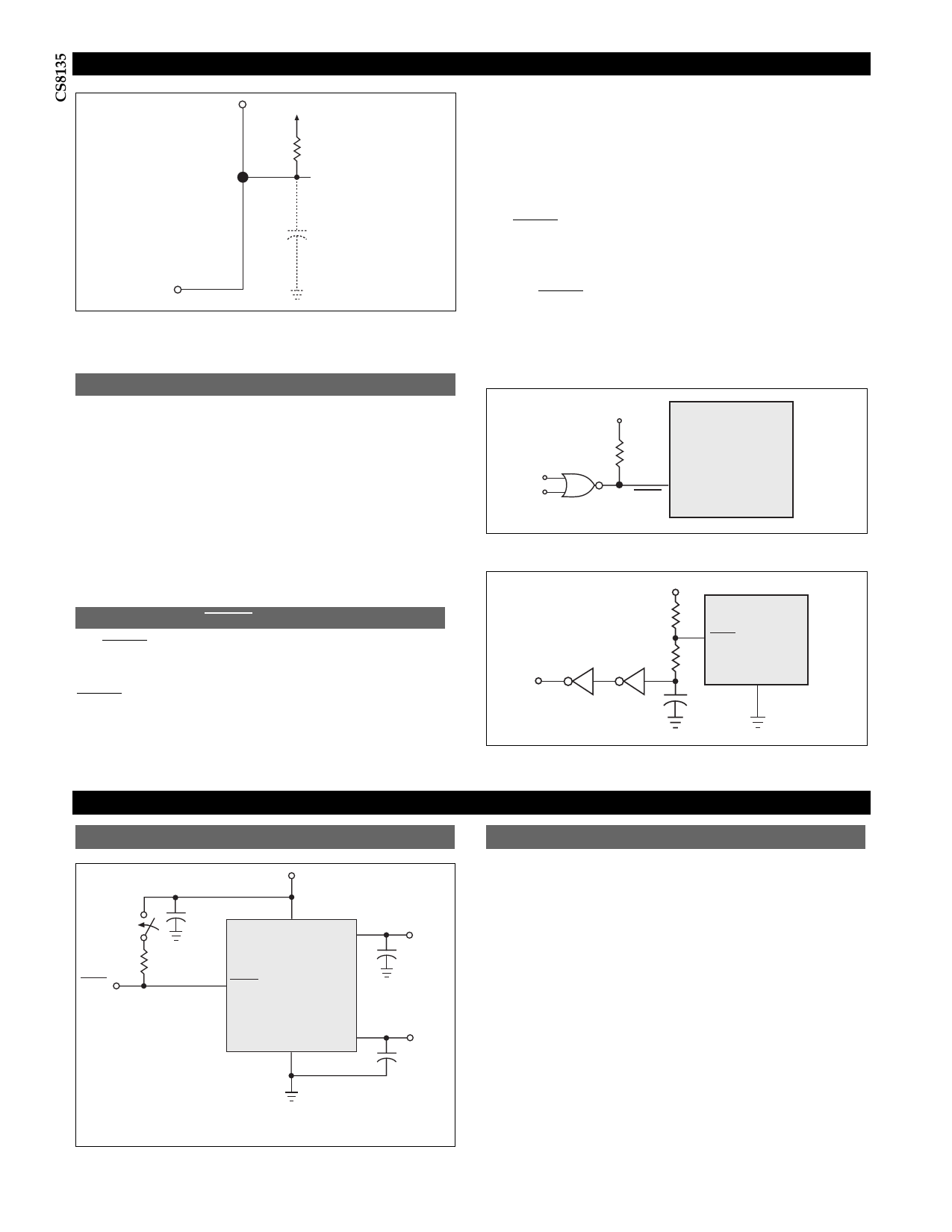
VOUT2
VIN
RD
10kW
VOUT2
+
C3
Disabling VOUT2 when it is not needed. C3 is no longer needed.
High Current Output
Unlike the standby regulated output, which must remain
on whenever possible, the high current regulated output is
fault protected against overvoltage and also incorporates
thermal shutdown. If the input voltage rises above approx-
imately 30V (e.g., load dump), this output will automatical-
ly shutdown. This protects the internal circuitry and
enables the IC to survive higher voltage transients than
would otherwise be expected. Thermal shutdown is effec-
tive against die overheating since the high current output
is the dominant source of power dissipation in the IC.
output voltage of this lead is high (5V). This is set by an
internal clamp. If the high current output becomes unreg-
ulated for any reason (line transients, short circuit, thermal
shutdown, low input voltage, etc.) the lead switches to the
active low state, and is capable of sinking several mil-
liamps. This output signal can be used to initiate any reset
or start-up procedure that may be required of the system.
The RESET lead can also be driven directly from logic cir-
cuits. The only requirement is that the 20k½ pull-up resis-
tor remain in place. This will not affect the logic gate since
the voltage on this lead is limited by the internal clamp to
5V. The RESET signal is sacrificed in this arrangement
since the maximum sink capability of the lead in the active
low state (approximately 5mA), is usually not sufficient to
pull down the active high logic gate. The flag can be
retained if the driving gate is open collector logic.
VIN
R1
20kW
RESET/
ENABLE
CS8135
Controlling ON/OFF Terminal with a typical CMOS or TTL Logic Gate
RESET Function
The RESET function has the ability to serve a dual purpose
if desired. When controlled in the manner shown in the
test circuit (common in automotive systems where
RESET /ENABLE is connected to the ignition switch), the
lead also serves as an output flag that is active low when-
ever a fault condition is detected with the high current
regulated output. Under normal operating conditions, the
Delayed
Reset
Out
CMOS MM 74CO4
or Equivalent
R1
20kW
CS8135
RESET/
ENABLE
R2
100kW
Gnd
4.7 mF
Reset Pulse on Power-Up (with approximately 300ms delay)
Application Notes
Test & Application Circuit
S1
ON/OFF
C1*
0.1 mF
R1
20kW
VIN
VOUT1
+
C2 **
10mF
RESET
FLAG
RESET/ CS8135
ENABLE
Gnd
VOUT2
+
C3**
10mF
NOTES:
* C1 required if regulator is located far from power supply filter.
** C2, C3 required for stability.
Stability Considerations
The output or compensation capacitor helps determine
three main characteristics of a linear regulator: start-up
delay, load transient response and loop stability.
The capacitor value and type should be based on cost,
availability, size and temperature constraints. A tantalum
or aluminum electrolytic capacitor is best, since a film or
ceramic capacitor with almost zero ESR, can cause insta-
bility. The aluminum electrolytic capacitor is the least
expensive solution, but, if the circuit operates at low tem-
peratures (-25¡C to -40¡C), both the value and ESR of the
capacitor will vary considerably. The capacitor manufac-
turers data sheet usually provides this information.
The value for output capacitor C2 shown in the test and
applications circuit should work for most applications,
however it is not necessarily the optimized solution.
To determine acceptable values for C2 and C3 for a partic-
ular application, start with a tantalum capacitor of the rec-
6
Share Link: 