CS51411G 데이터 시트보기 (PDF) - ON Semiconductor
부품명
상세내역
일치하는 목록
CS51411G Datasheet PDF : 20 Pages
| |||
CS51411, CS51412, CS51413, CS51414
The power dissipated by the IC due to this current is
WBASE
+
VO2
VIN
IS
60
where:
IS = DC switching current.
When the power switch turns on, the saturation voltage
and conduction current contribute to the power loss of a
non-ideal switch. The power loss can be quantified as
WSAT
+
VO
VIN
IS
VSAT
where:
VSAT = saturation voltage of the power switch which is
shown in Figure 12.
The switching loss occurs when the switch experiences
both high current and voltage during each switch transition.
This regulator has a 30 ns turn-off time and associated
power loss is equal to
WS + IS
VIN
2
30Ăns
fS
The turn-on time is much shorter and thus turn-on loss is
not considered here.
The total power dissipated by the IC is sum of all the above
WIC + WQ ) WDRV ) WBASE ) WSAT ) WS
The IC junction temperature can be calculated from the
ambient temperature, IC power dissipation and thermal
resistance of the package. The equation is shown as follows,
TJ + WIC RqJA ) TA
The maximum IC junction temperature shall not exceed
125°C to guarantee proper operation and avoid any damages
to the IC.
Using the BIAS Pin
The efficiency savings in using the BIAS pin is most
notable at low load and high input voltage as will be
explained below.
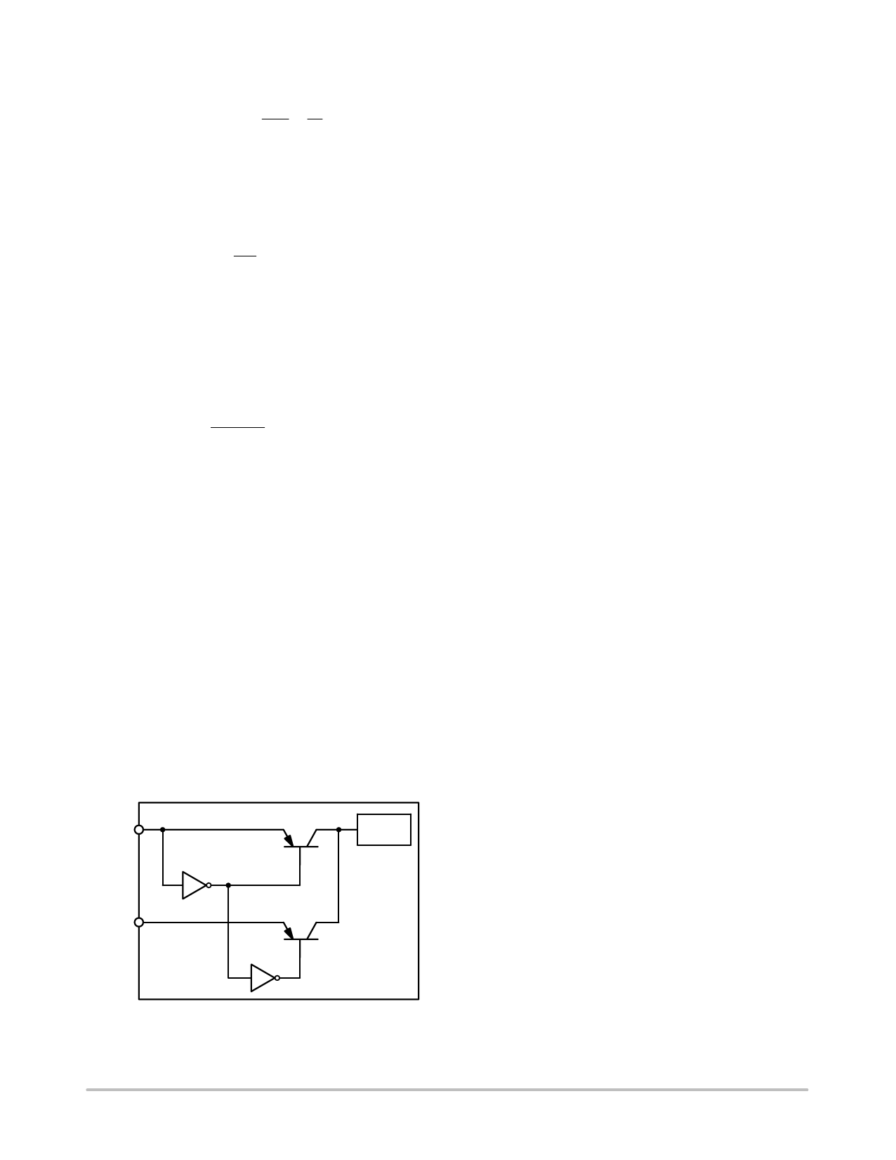
Figure 17 will help to understand the increase in efficiency
when the BIAS pin is used. The circuitry shown is not the
actual implementation, but is useful in the explanation.
BIAS
P1
Internal
BIAS
Vin
P2
Internal bias to the IC can be supplied via the Vin pin or the
BIAS pin. When the BIAS pin is low, the logic turns P2 on
and current is routed to the internal bias circuitry from the
Vin pin. Conversely, when the BIAS pin is high, the logic
turns P1 on and current is routed to the internal bias circuitry
from the BIAS pin.
Here is an example of the power savings:
The input voltage range for Vin is 4.5 V to 40 V. The input
voltage range for BIAS is 3.3 V to 6 V. The quiescent current
specification is 3 mA (min), 4 mA (typ), and 6.25 mA (max).
Using a typical battery voltage of 14 V and the typical
quiescent current number of 4 mA, the power would be:
P + V I + 14 4e-3 + 56ĂmW
We'll assume the BIAS pin is connected to an external
regulator at 5 V instead of the output voltage. The BIAS pin
would normally be connected to the output voltage, but
adding an added switching regulator efficiency number here
would cloud this example. Now the internal BIAS circuitry
is being powered via 5 V. The resulting on chip power being
dissipated is:
P + V I + 5 4e-3 + 21ĂmW
The power savings is 35 mW.
Now, to demonstrate more notable savings using the
maximum battery input voltage of 40 V, the maximum
quiescent current of 6.25 mA, and the lowest allowed BIAS
voltage for proper operation of 3.3 V;
Powered from Vin:
P + 40 6.25e-3 + 250ĂmW
Powered from the BIAS pin:
P + 3.3 6.25e-3 + 21ĂmW
The power savings is 229 mW.
Minimum Load Requirement
As pointed out in the previous section, a minimum load is
required for this regulator due to the predriver current
feeding the output. Placing a resistor equal to VO divided by
12 mA should prevent any voltage overshoot at light load
conditions. Alternatively, the feedback resistors can be
valued properly to consume 12 mA current.
COMPONENT SELECTION
Input Capacitor
In a buck converter, the input capacitor witnesses pulsed
current with an amplitude equal to the load current. This
pulsed current and the ESR of the input capacitors determine
the VIN ripple voltage, which is shown in Figure 18. For VIN
ripple, low ESR is a critical requirement for the input
capacitor selection. The pulsed input current possesses a
significant AC component, which is absorbed by the input
capacitors.
Figure 17.
http://onsemi.com
12
Share Link: 