CS51411(2002) 데이터 시트보기 (PDF) - ON Semiconductor
부품명
상세내역
일치하는 목록
CS51411
(Rev.:2002)
(Rev.:2002)
ON Semiconductor

CS51411 Datasheet PDF : 16 Pages
| |||
CS51411, CS51412, CS51413, CS51414
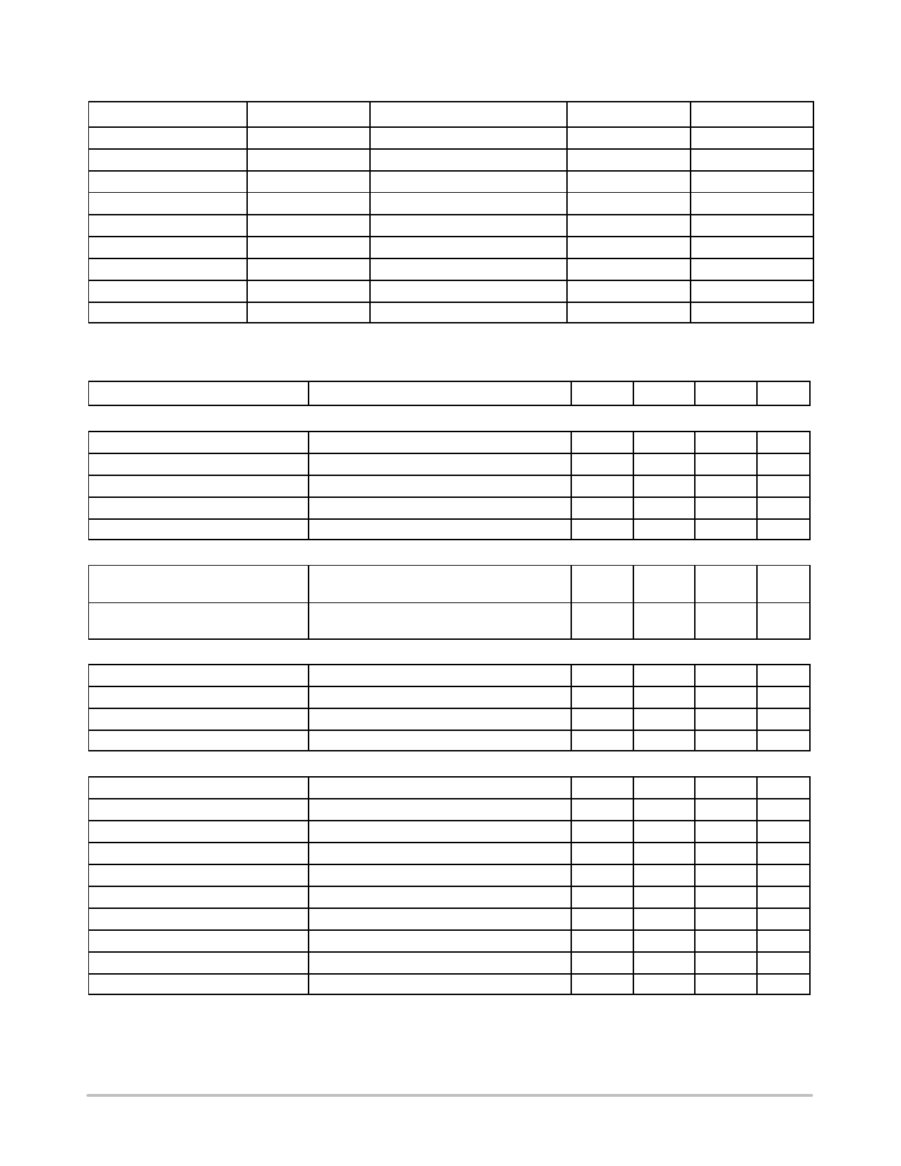
ELECTRICAL CHARACTERISTICS (continued) (–40°C < TJ < 125°C (CS51411E/2E/3E/4E); –40°C < TA < 85°C (CS51411E/2E/3E/4E);
0°C < TA < 70°C (CS51411G/2G/3G/4G), 4.5 V< VIN < 40 V; unless otherwise specified.)
Characteristic
Test Conditions
Min
Typ
Max
Unit
Sync
Sync Frequency Range
CS51411/CS51412
305
–
470
kHz
Sync Frequency Range
CS51413/CS51414
575
–
880
kHz
Sync Pin Bias Current
Sync Threshold Voltage
VSYNC = 0 V
VSYNC = 5.0 V
–
–
0.1
0.2
µA
250
360
460
µA
1.0
1.5
1.9
V
Shutdown
Shutdown Threshold Voltage
–
1.0
1.3
1.6
V
Shutdown Pin Bias Current
Thermal Shutdown
Overtemperature Trip Point
VSHDNB = 0 V
Note 3
0.14
5.00
35
µA
175
185
195
°C
Thermal Shutdown Hysteresis
Note 3
–
42
–
°C
General
Quiescent Current
Shutdown Quiescent Current
Boost Operating Current
Minimum Boost Voltage
ISW = 0 A
VSHDNB = 0 V
VBOOST – VSW = 2.5 V
Note 3
3.0
4.0
6.25
mA
8.0
20
85
µA
6.0
15
40
mA/A
–
–
2.5
V
Start up Voltage
–
2.2
3.3
4.4
V
Minimum Output Current
–
–
7.0
12
mA
3. Guaranteed by design, not 100% tested in production.
PACKAGE PIN DESCRIPTION
PACKAGE PIN #
PIN SYMBOL
1
BOOST
2
VIN
3
VSW
4 (CS51412/CS51414)
5 (CS51411/CS51413)
5 (CS51412/CS51414)
4 (CS51411/CS51413)
6
7
BIAS
SYNC
SHDNB
GND
VFB
8
VC
FUNCTION
The BOOST pin provides additional drive voltage to the on–chip NPN power transistor.
The resulting decrease in switch on voltage increases efficiency.
This pin is the main power input to the IC.
This is the connection to the emitter of the on–chip NPN power transistor and serves
as the switch output to the inductor. This pin may be subjected to negative voltages
during switch off–time. A catch diode is required to clamp the pin voltage in normal
operation. This node can stand –1.0 V for less than 50 ns during switch node flyback.
The BIAS pin connects to the on–chip power rail and allows the IC to run most of its
internal circuitry from the regulated output or another low voltage supply to improve
efficiency. The BIAS pin is left floating if this feature is not used.
This pin provides the synchronization input.
The shutdown pin is active low and TTL compatible. The IC goes into sleep mode,
drawing less than 85 µA when the pin voltage is pulled below 1.0 V. This pin should be
left floating in normal position.
Power return connection for the IC.
The FB pin provides input to the inverting input of the error amplifier. If VFB is lower
than 0.29 V, the oscillator frequency is divided by four, and current limit folds back to
about 1 ampere. These features protect the IC under severe overcurrent or short
circuit conditions.
The VC pin provides a connection point to the output of the error amplifier and input to
the PWM comparator. Driving of this pin should be avoided because on–chip test
circuitry becomes active whenever current exceeding 0.5 mA is forced into the IC.
http://onsemi.com
4
Share Link: