CRX14 데이터 시트보기 (PDF) - STMicroelectronics
부품명
상세내역
일치하는 목록
CRX14 Datasheet PDF : 40 Pages
| |||
CRX14
If a CRC error is detected, the Status Slot Bit is set
to ‘0’, and the corresponding Slot_Register is set
to FFh.
Each time the Slot Marker Register is accessed in
I²C Write mode, Byte 0 of the Input/Output Frame
Register is set to 18, Bytes 1 and 2 provide Status
Bits Slot information, and Bytes 3 to 18 store the
corresponding Chip_ID or error code.
The Slot Marker Register cannot be accessed in
I²C Read mode. All the anti-collision data can be
accessed by reading the Input/Output Frame Reg-
ister at the I²C address 01h.
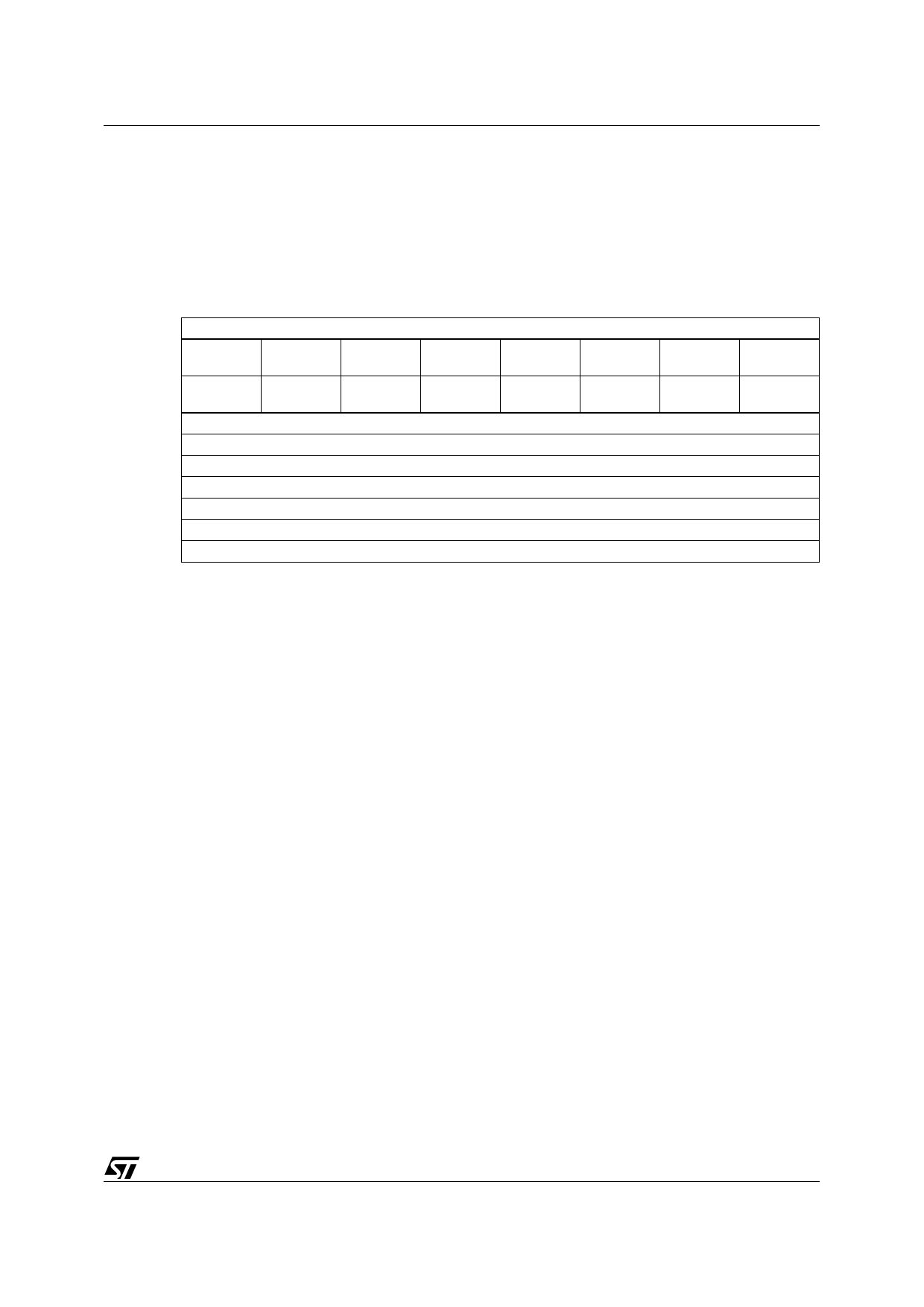
Table 5. Slot Marker Register Description
b7
b6
b5
b4
b3
b2
b1
Byte 0
Number of stored Bytes: fixed to 18
Byte 1
Status Slot Status Slot Status Slot Status Slot Status Slot Status Slot Status Slot
Bit 7
Bit 6
Bit 5
Bit 4
Bit 3
Bit 2
Bit 1
Byte 2
Status Slot Status Slot Status Slot Status Slot Status Slot Status Slot Status Slot
Bit 15
Bit 14
Bit 13
Bit 12
Bit 11
Bit 10
Bit 9
Byte 3
Slot_Register 0 = Chip_ID value detected in Slot 0
Byte 4
Slot_Register 1 = Chip_ID value detected in Slot 1
Byte 5
Slot_Register 2 = Chip_ID value detected in Slot 2
Byte 6
Slot_Register 3 = Chip_ID value detected in Slot 3
Byte n
.....
Byte 17
Slot_Register 14 = Chip_ID value detected in Slot 14
Byte 18
Slot_Register 15 = Chip_ID value detected in Slot 15
Status bit value description:
1: No error detected. The Chip_ID stored in the Slot register is valid.
0: Error detected
- Slot register = 00h: No answer frame detected from ST short range memory
- Slot register = FFh: Answer Frame detected with CRC error. Collision may have occurred
b0
Status Slot
Bit 0
Status Slot
Bit 8
11/40
Share Link: 