CMX882 데이터 시트보기 (PDF) - CML Microsystems Plc
부품명
상세내역
일치하는 목록
CMX882 Datasheet PDF : 70 Pages
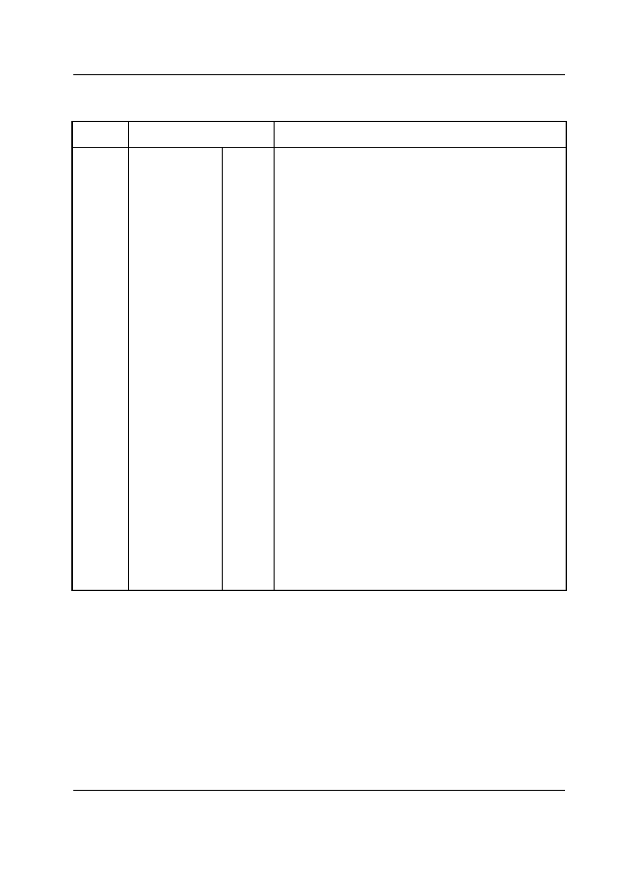
| |||
FRS Signalling Processor
CMX882
1.3 Signal List (continued)
Package
D6, E1
Pin No.
10
11
12
13
14
15
16
17
19
20
22
24
25
26
27, 28
Signal
Name
VBIAS
DISC
DISC_FB
INPUT_2
INPUT_2_FB
MIC
MIC_FB
SIG_MONITOR
MOD_1
MOD_2
AUDIO
CLOCK/XTAL
CLOCK_OUT
Type
O/P
I/P
O/P
I/P
O/P
I/P
O/P
I/P
O/P
O/P
O/P
I/P
O/P
I/P
NC
Description
Internally generated bias voltage of approximately VDD(A)/2,
except when bias is power-saved when VBIAS will discharge
to VSS(A). This pin should be decoupled to VSS(A) by a
capacitor mounted close to the device pins.
Input terminal of discriminator input amplifier.
Output / feedback terminal of discriminator input amplifier.
Input terminal of amplifier 2, for either a second microphone
or discriminator input.
Output / feedback terminal of input amplifier 2.
Input terminal of microphone input amplifier.
Output / feedback terminal of microphone input amplifier.
Signal Monitor input to the internal level detecting circuit.
Modulator 1 output.
Modulator 2 output.
Output of the audio section.
The input to the on-chip oscillator for an external crystal or a
clock circuit.
Buffered (un-inverted) clock output available for use by
other devices in the system.
Test input, connect to VSS(D).
No connection should be made to these pins.
Notes: I/P =
O/P =
T/S =
NC =
Input
Output
3-state Output
No Connection
2004 CML Microsystems Plc
10
D/882/7
Share Link: 