CM150RX-24S 데이터 시트보기 (PDF) - Powerex
부품명
상세내역
일치하는 목록
CM150RX-24S Datasheet PDF : 13 Pages
| |||
Powerex, Inc., 173 Pavilion Lane, Youngwood, Pennsylvania 15697 (724) 925-7272 www.pwrx.com
CM150RX-24S
Six IGBT + Brake NX-Series Module
150 Amperes/1200 Volts
Electrical Characteristics, Tj = 25°C unless otherwise specified
Inverter Part IGBT/FWDi
Characteristics
Symbol
Test Conditions
Min.
Typ. Max.
Collector-Emitter Cutoff Current
ICES
VCE = VCES, VGE = 0V
—
—
1.0
Gate-Emitter Leakage Current
IGES
VGE = VGES, VCE = 0V
—
—
0.5
Gate-Emitter Threshold Voltage
VGE(th)
IC = 15mA, VCE = 10V
5.4
6.0
6.6
Collector-Emitter Saturation Voltage
VCE(sat)
IC = 150A, VGE = 15V, Tj = 25°C*5
—
1.80
2.25
(Terminal)
IC = 150A, VGE = 15V, Tj = 125°C*5
—
2.00
—
IC = 150A, VGE = 15V, Tj = 150°C*5
—
2.05
—
Collector-Emitter Saturation Voltage
VCE(sat)
IC = 150A, VGE = 15V, Tj = 25°C*5
—
1.70
2.15
(Chip)
IC = 150A, VGE = 15V, Tj = 125°C*5
—
1.90
—
IC = 150A, VGE = 15V, Tj = 150°C*5
—
1.95
—
Input Capacitance
Cies
—
—
15
Output Capacitance
Coes
VCE = 10V, VGE = 0V
—
—
3.0
Reverse Transfer Capacitance
Cres
—
—
0.25
Gate Charge
QG
VCC = 600V, IC = 150A, VGE = 15V
—
350
—
Turn-on Delay Time
td(on)
—
—
800
Rise Time
tr
VCC = 600V, IC = 150A, VGE = ±15V,
—
—
200
Turn-off Delay Time
td(off)
RG = 0Ω, Inductive Load
—
—
600
Fall Time
tf
—
—
300
Emitter-Collector Voltage
VEC*1
IE = 150A, VGE = 0V, Tj = 25°C*5
—
1.80
2.25
(Terminal)
IE = 150A, VGE = 0V, Tj = 125°C*5
—
1.80
—
IE = 150A, VGE = 0V, Tj = 150°C*5
—
1.80
—
Emitter-Collector Voltage
VEC*1
IE = 150A, VGE = 0V, Tj = 25°C*5
—
1.70
2.15
(Chip)
IE = 150A, VGE = 0V, Tj = 125°C*5
—
1.70
—
IE = 150A, VGE = 0V, Tj = 150°C*5
—
1.70
—
Reverse Recovery Time
trr*1
VCC = 600V, IE = 150A, VGE = ±15V
—
—
300
Reverse Recovery Charge
Qrr*1
RG = 0Ω, Inductive Load
—
8.0
—
Turn-on Switching Energy per Pulse
Eon
VCC = 600V, IC = IE = 150A,
—
24.2
—
Turn-off Switching Energy per Pulse
Eoff
VGE = ±15V, RG = 0Ω,
—
16
—
Reverse Recovery Energy per Pulse
Err*1
Tj = 150°C, Inductive Load
—
12.2
—
Internal Lead Resistance
RCC' + EE'
Main Terminals-Chip,
—
—
1.8
Per Switch,TC = 25°C*4
Internal Gate Resistance
rg
Per Switch
—
13
—
*1 Represent ratings and characteristics of the anti-parallel, emitter-to-collector free wheeling
diode (FWDi).
*4 Case temperature (TC) and heatsink temperature (Ts) is measured on the surface
(mounting side) of the baseplate and the heatsink side just under the chips.
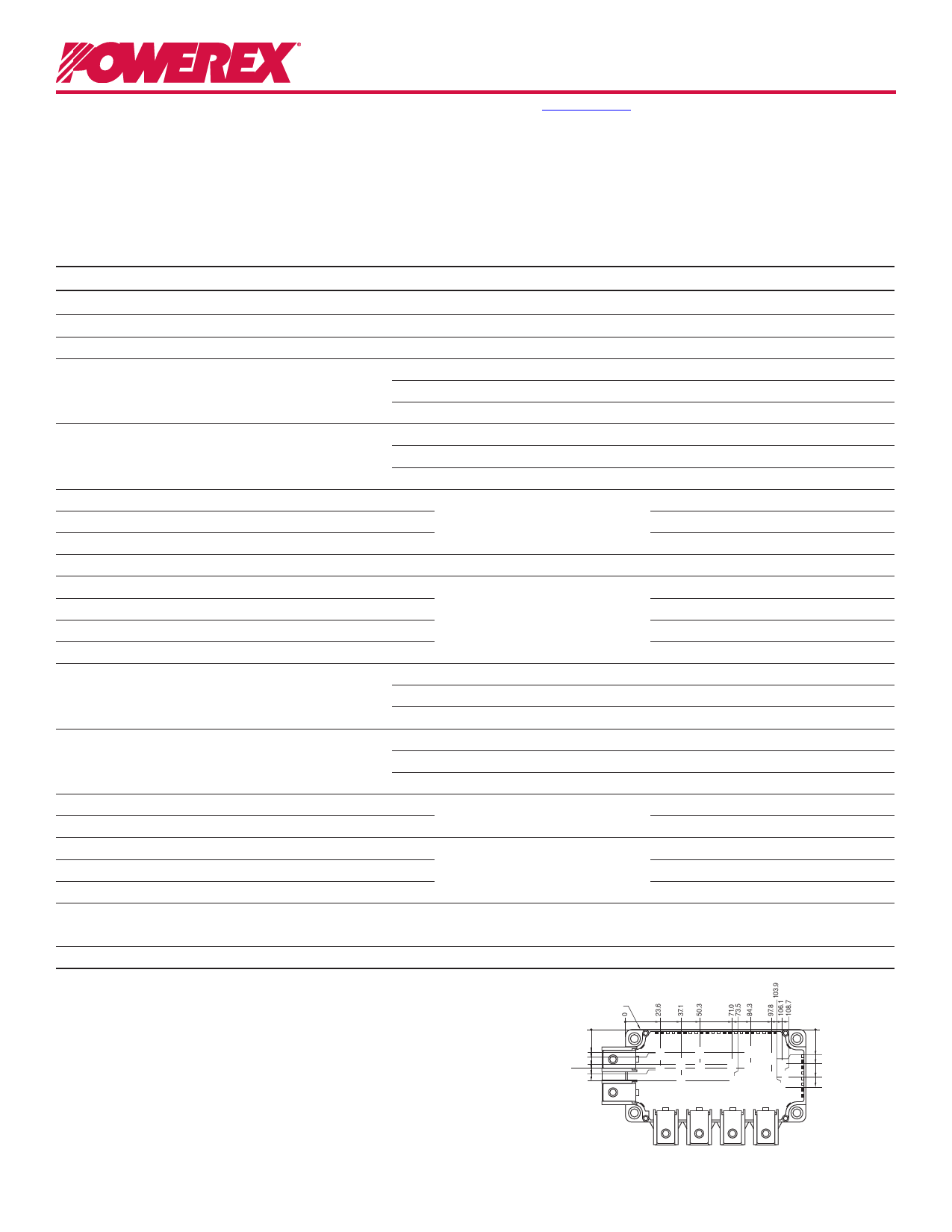
Refer to the figure to the right for chip location.
The heatsink thermal resistance should be measured just under the chips.
*5 Pulse width and repetition rate should be such as to cause negligible temperature rise.
LABEL SIDE
0
15.3
17.6
26.0 22.6
28.4
34.4
34 33 32 31 30 29 28 27 26 25 24 23 22 21 20 19 18 17 16 15 14 13
Tr
35 UP
Di
UP
36
Tr
VP
Tr
UN Di
VP
Di
UN
1
2
Tr
WP
Tr
VN
Di
WP
Di
VN
3
Tr
12
WN Th 11
10
Di Di 9
WN Br 8
Tr
7
Br 6
5
4
0
21.5
22.7
32.3
42.8
Units
mA
µA
Volts
Volts
Volts
Volts
Volts
Volts
Volts
nF
nF
nF
nC
ns
ns
ns
ns
Volts
Volts
Volts
Volts
Volts
Volts
ns
µC
mJ
mJ
mJ
mΩ
Ω
03/13 Rev. 5
Each mark points to the center position of each chip.
Tr*P / Tr*N / TrBr (* = U/V/W): IGBT Di*P / Di*N (* = U/V/W): FWDi
DiBr: Clamp
Th: NTC Thermistor
3
Share Link: 