CD4010CN 데이터 시트보기 (PDF) - Fairchild Semiconductor
부품명
상세내역
일치하는 목록
CD4010CN Datasheet PDF : 5 Pages
| |||
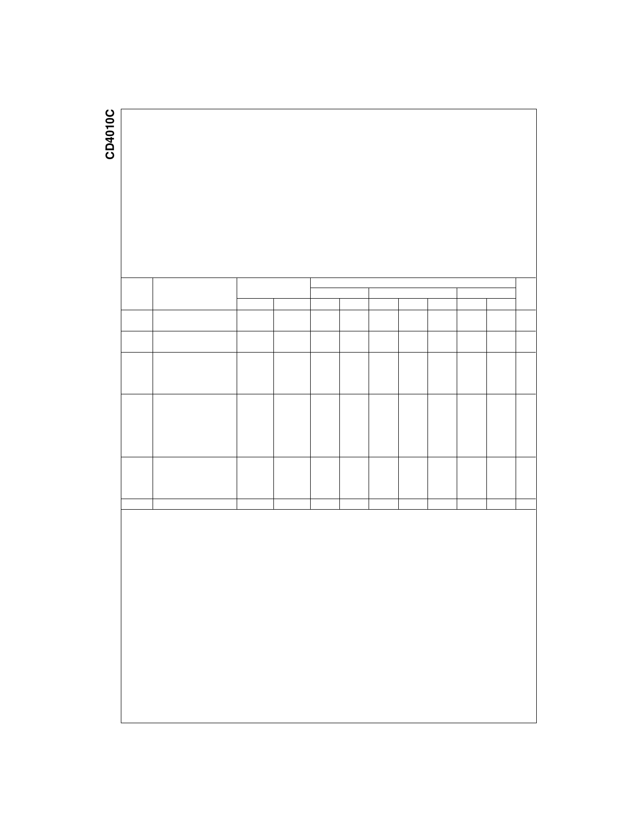
Absolute Maximum Ratings(Note 1)
Voltage at Any Pin (Note 2)
Operating Temperature Range
VSS − 0.3V to VSS +15.5V
−45°C to +85°C
Storage Temperature Range (TS)
Power Dissipation (PD)
Dual-In-Line
−65°C to +150°C
700 mW
Small Outline
500 mW
Lead Temperature (TL)
(Soldering, 10 seconds)
260°C
Operating Range (VDD)
VSS + 3V to VSS + 15V
Note 1: “Absolute Maximum Ratings indicate limits beyond which damage
to the device may occur. Operating Ratings indicate conditions for which
the device is functional, but do not guarantee specific performance limits.”
Note 2: This device should not be connected to circuits with the power on
because high transient voltage may cause permanent damage.
DC Electrical Characteristics
Test Conditions
Symbol
Characteristics
(Volts)
VO
VDD
ICC
Quiescent Device
5
Current
10
PD
Quiescent Device
5
Dissipation/Package
10
Output Voltage
5
VOL
LOW Level
10
VOH
HIGH Level
5
10
Noise Immunity
(All Inputs)
VNL
VNH
Output Drive Current
VO ≥ 1.5
5
VO ≥ 3.0
10
VO ≥ 3.5
5
VO ≥ 7.0
10
0.4
5
IDN
N-Channel (Note 3)
IDP
P-Channel (Note 3)
0.5
10
2.5
5
9.5
10
IIN
Input Current
Note 3: IDN and IDP are tested one output at a time.
−40°C
Min
Max
3
5
15
50
0.01
0.01
4.99
9.99
Limits
+25°C
Min
Typ
Max
0.03
3
0.05
5
0.15
15
0.5
50
0
0.01
0
0.01
4.99
5
9.99
10
+85°C
Min
Max
42
70
210
700
0.05
0.05
4.95
9.95
Units
µA
µA
µW
µW
V
V
V
V
1.6
3.2
1.4
2.9
3.6
9.6
−1.5
−0.72
1.5
2.25
3
4.5
1.5
2.25
3
4.5
3
8
−1.25
−0.6
10
1.4
V
2.9
V
1.5
V
3
V
2.4
mA
6.4
mA
−1
mA
−0.48
mA
pA
www.fairchildsemi.com
2
Share Link: 