CBT6810DK 데이터 시트보기 (PDF) - Philips Electronics
부품명
상세내역
일치하는 목록
CBT6810DK
Philips Electronics

CBT6810DK Datasheet PDF : 9 Pages
| |||
Philips Semiconductors
10-bit bus switch with precharged outputs
and Schottky undershoot protection for live insertion
Product data
CBT6810
FEATURES
• 5 Ω switch connection between port A and port B
• TTL compatible input and output levels
• Undershoot protection included to prevent shoot through level
changes
• Bias voltage pre-charges the outputs to minimize signal distortion
during live insertion
• Latch-up protection exceeds 500 mA per JESD78
• ESD protection exceeds 2000 V HBM per JESD22-A114,
200 V MM per JESD22-A115 and 1000 V CDM per JESD22-C101
DESCRIPTION
The CBT6810 provides ten bits of high-speed TTL-compatible bus
switching. The low on-state resistance of the switch allows
bi-directional connections to be made while adding near-zero
propagation delay. The device also precharges the B port to a
user-selectable bias voltage (BIASV) to minimize live-insertion
noise.
The CBT6810 is organized as one 10-bit switch with a single enable
(OE) input. When OE is low, the switch is on and port A is
connected to port B. When OE is high, the switch between port A
and port B is open and the B port is precharged to BIASV through
the equivalent of a 10-kΩ resistor.
The CBT6810 is characterized for operation from -40 to +85 °C.
QUICK REFERENCE DATA
SYMBOL
PARAMETER
tPLH
Propagation delay
tPHL
An to Bn or Bn to An
CIN
Input capacitance
CIO
Input/output capacitance
CONDITIONS
Tamb = 25 °C; GND = 0 V
CL = 50 pF; VCC = 5 V
VI = 0 V or VCC
Outputs disabled; VO = 0 V or VCC
TYPICAL
250
3.5
9.0
UNIT
ps
pF
pF
ORDERING INFORMATION
PACKAGES
24-Pin Plastic TSSOP
24-Pin Plastic SSOP (QSOP)
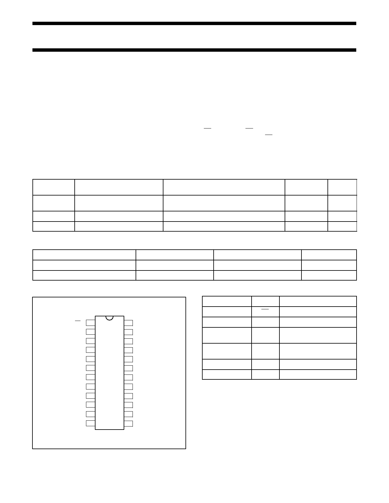
PIN CONFIGURATION
OE 1
A1 2
A2 3
A3 4
A4 5
A5 6
A6 7
A7 8
A8 9
A9 10
A10 11
GND 12
TEMPERATURE RANGE
-40 to +85 °C
-40 to +85 °C
ORDER CODE
CBT6810PW
CBT6810DK
DWG NUMBER
SOT355-1
SOT556-1
24 Vcc
23 B1
22 B2
21 B3
20 B4
19 B5
18 B6
17 B7
16 B8
15 B9
14 B10
13 BIASV
PIN DESCRIPTION
PIN NUMBER SYMBOL
NAME AND FUNCTION
1
OE Output enable
13
BIASV Precharge bias voltage input
2, 3, 4, 5, 6,
7, 8, 9, 10, 11
A1-A10 A - port side
23, 22, 21, 20, 19,
18, 17, 16, 15, 14
B1-B10
B - port side with active pullup
12
GND Ground (V)
24
VCC Positive supply voltagem
SA00505
2002 Dec 13
2
Share Link: