CAT24C16HU4I-GT3(2013) 데이터 시트보기 (PDF) - ON Semiconductor
부품명
상세내역
일치하는 목록
CAT24C16HU4I-GT3 Datasheet PDF : 21 Pages
| |||
CAT24C01, CAT24C02, CAT24C04, CAT24C08, CAT24C16
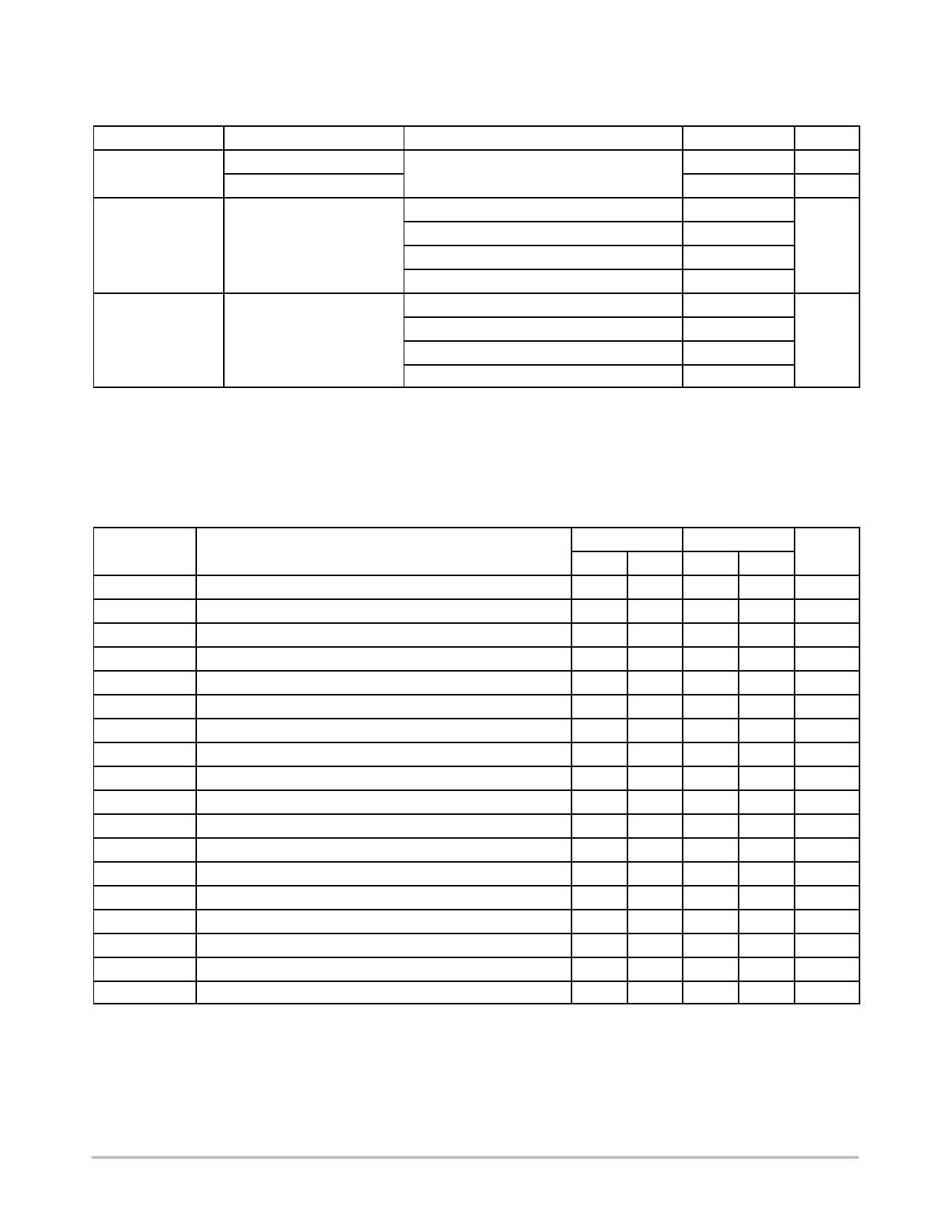
Table 5. PIN IMPEDANCE CHARACTERISTICS
(VCC = 1.8 V to 5.5 V, TA = −40°C to +125°C and VCC = 1.7 V to 5.5 V, TA = −40°C to +85°C, unless otherwise specified.)
Symbol
Parameter
Conditions
Max
Units
CIN (Note 4)
SDA Pin Capacitance
Other Pins
VIN = 0 V, f = 1.0 MHz, VCC = 5.0 V
8
pF
6
pF
IWP (Note 5)
WP Input Current
VIN < VIH, VCC = 5.5 V
130
mA
VIN < VIH, VCC = 3.3 V
120
VIN < VIH, VCC = 1.7 V
80
VIN > VIH
2
IA (Note 5)
Address Input Current
(A0, A1, A2)
Product Rev H: CAT24C02
Product Rev K: CAT24C04,
CAT24C08, CAT24C16
VIN < VIH, VCC = 5.5 V
VIN < VIH, VCC = 3.3 V
VIN < VIH, VCC = 1.7 V
VIN > VIH
50
mA
35
25
2
4. These parameters are tested initially and after a design or process change that affects the parameter according to appropriate AEC−Q100
and JEDEC test methods.
5. When not driven, the WP, A0, A1 and A2 pins are pulled down to GND internally. For improved noise immunity, the internal pull−down is
relatively strong; therefore the external driver must be able to supply the pull−down current when attempting to drive the input HIGH. To
conserve power, as the input level exceeds the trip point of the CMOS input buffer (~ 0.5 x VCC), the strong pull−down reverts to a weak
current source.
Table 6. A.C. CHARACTERISTICS
(Note 6) (VCC = 1.8 V to 5.5 V, TA = −40°C to +125°C and VCC = 1.7 V to 5.5 V, TA = −40°C to +85°C, unless otherwise specified.)
Standard
Fast
Symbol
Parameter
Min
Max
Min
Max
Units
FSCL
tHD:STA
tLOW
tHIGH
tSU:STA
tHD:DAT
tSU:DAT
tR
Clock Frequency
START Condition Hold Time
Low Period of SCL Clock
High Period of SCL Clock
START Condition Setup Time
Data In Hold Time
Data In Setup Time
SDA and SCL Rise Time
100
400
kHz
4
0.6
ms
4.7
1.3
ms
4
0.6
ms
4.7
0.6
ms
0
0
ms
250
100
ns
1000
300
ns
tF (Note 6)
tSU:STO
tBUF
tAA
tDH
Ti (Note 6)
tSU:WP
tHD:WP
tWR
SDA and SCL Fall Time
STOP Condition Setup Time
Bus Free Time Between STOP and START
SCL Low to Data Out Valid
Data Out Hold Time
Noise Pulse Filtered at SCL and SDA Inputs
WP Setup Time
WP Hold Time
Write Cycle Time
300
300
ns
4
0.6
ms
4.7
1.3
ms
3.5
0.9
ms
100
100
ns
100
100
ns
0
0
ms
2.5
2.5
ms
5
5
ms
tPU (Notes 7, 8) Power−up to Ready Mode
1
6. Test conditions according to “AC Test Conditions” table.
7. Tested initially and after a design or process change that affects this parameter.
8. tPU is the delay between the time VCC is stable and the device is ready to accept commands.
1
ms
http://onsemi.com
3
Share Link: 