OM5232 데이터 시트보기 (PDF) - Philips Electronics
부품명
상세내역
일치하는 목록
OM5232 Datasheet PDF : 11 Pages
| |||
Philips Semiconductors
CMOS single-chip 8-bit microcontroller
Product specification
OM5232
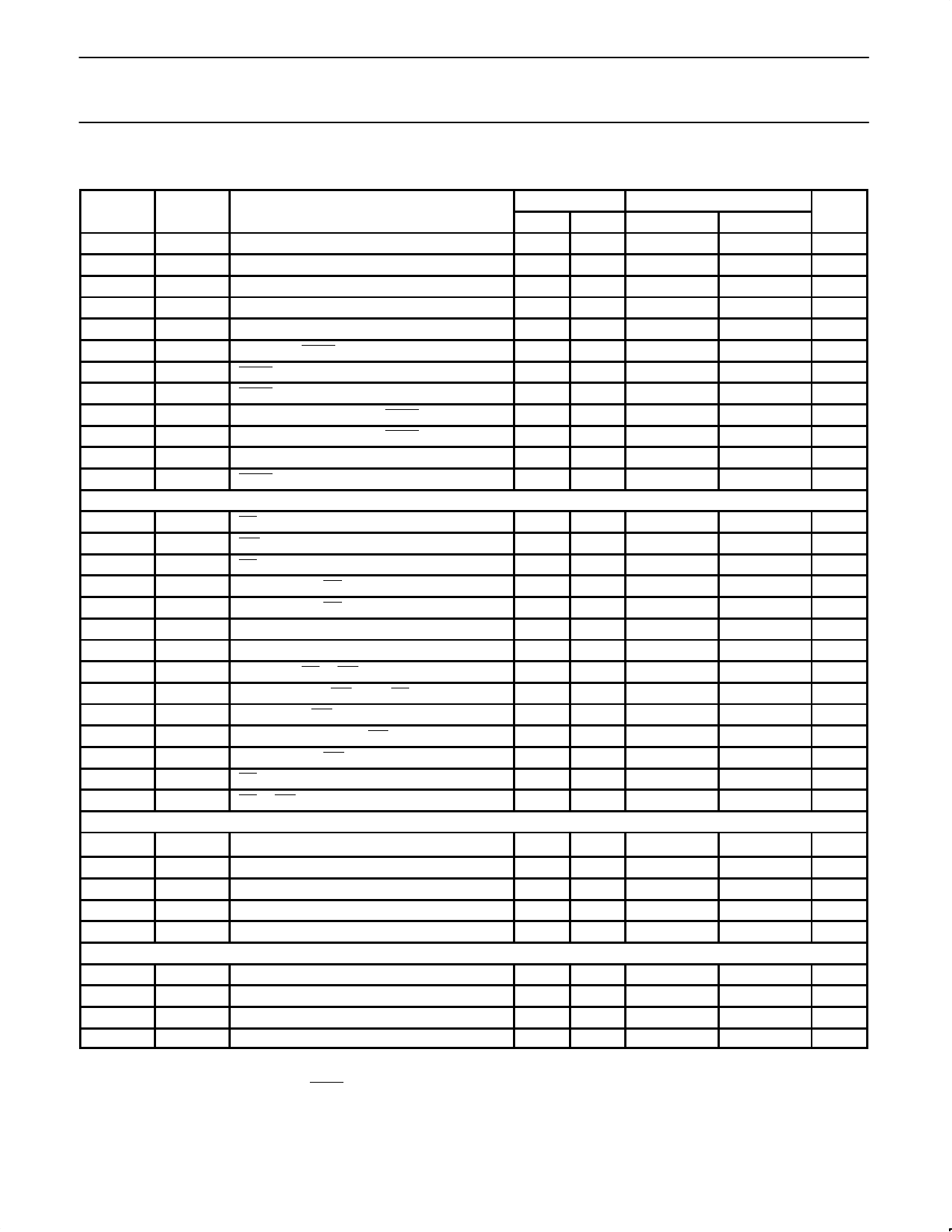
AC ELECTRICAL CHARACTERISTICS1, 2
16MHz CLOCK
VARIABLE CLOCK
SYMBOL FIGURE
PARAMETER
MIN MAX
MIN
MAX
1/tCLCL
2
tLHLL
2
tAVLL
2
tLLAX
2
tLLIV
2
tLLPL
2
tPLPH
2
tPLIV
2
tPXIX
2
tPXIZ
2
tAVIV
2
tPLAZ
2
Data Memory
Oscillator frequency
ALE pulse width
Address valid to ALE low
Address hold after ALE low
ALE low to valid instruction in
ALE low to PSEN low
PSEN pulse width
PSEN low to valid instruction in
Input instruction hold after PSEN
Input instruction float after PSEN
Address to valid instruction in
PSEN low to address float
1.2
16
85
2tCLCL–40
8
tCLCL–55
28
tCLCL–35
150
4tCLCL–100
23
tCLCL–40
143
3tCLCL–45
83
3tCLCL–105
0
0
38
tCLCL–25
208
5tCLCL–105
10
10
tRLRH
3, 4
RD pulse width
275
6tCLCL–100
tWLWH
tRLDV
3, 4
WR pulse width
3, 4
RD low to valid data in
275
6tCLCL–100
148
tRHDX
3, 4
Data hold after RD
0
0
tRHDZ
3, 4
Data float after RD
55
tLLDV
3, 4
ALE low to valid data in
350
tAVDV
3, 4
Address to valid data in
398
tLLWL
tAVWL
3, 4
ALE low to RD or WR low
3, 4
Address valid to WR low or RD low
138
238
3tCLCL–50
120
4tCLCL–130
tQVWX
3, 4
Data valid to WR transition
3
tCLCL–60
tDW
3, 4
Data setup time before WR
288
7tCLCL–150
tWHQX
3, 4
Data hold after WR
13
tCLCL–50
tRLAZ
tWHLH
3, 4
RD low to address float
3, 4
RD or WR high to ALE high
0
23
103
tCLCL–40
Shift Register
tXLXL
tQVXH
tXHQX
tXHDX
tXHDV
5
Serial port clock cycle time3
5
Output data setup to clock rising edge3
5
Output data hold after clock rising edge3
5
Input data hold after clock rising edge3
5
Clock rising edge to input data valid3
0.75
492
80
0
12tCLCL
10tCLCL–133
2tCLCL–117
0
492
External Clock
tCHCX
6
High time3
20
20
tCLCX
6
Low time3
20
20
tCLCH
6
Rise time3
20
tCHCL
6
Fall time3
20
NOTES:
1. Parameters are valid over operating temperature range unless otherwise specified.
2. Load capacitance for port 0, ALE, and PSEN = 100pF, load capacitance for all other outputs = 80pF.
3. These values are characterized but not 100% production tested.
5tCLCL–165
2tCLCL–70
8tCLCL–150
9tCLCL–165
3tCLCL+50
0
tCLCL+40
10tCLCL–133
tCLCL – tCLCX
tCLCL – tCHCX
20
20
UNIT
MHz
ns
ns
ns
ns
ns
ns
ns
ns
ns
ns
ns
ns
ns
ns
ns
ns
ns
ns
ns
ns
ns
ns
ns
ns
ns
µs
ns
ns
ns
ns
ns
ns
ns
ns
December 1994
8
Share Link: 