PI3B3244 데이터 시트보기 (PDF) - Pericom Semiconductor
부품명
상세내역
일치하는 목록
PI3B3244 Datasheet PDF : 5 Pages
| |||
PI3B3244
3.3V, Hot Insertion
1234567890123456789012345678901212345678901234567890123456789012123456789012345678901234567890121234567889-0B12i3t4,5627-8P90o12r3t45N67a89n0o12S12w34i5tc67h89™012
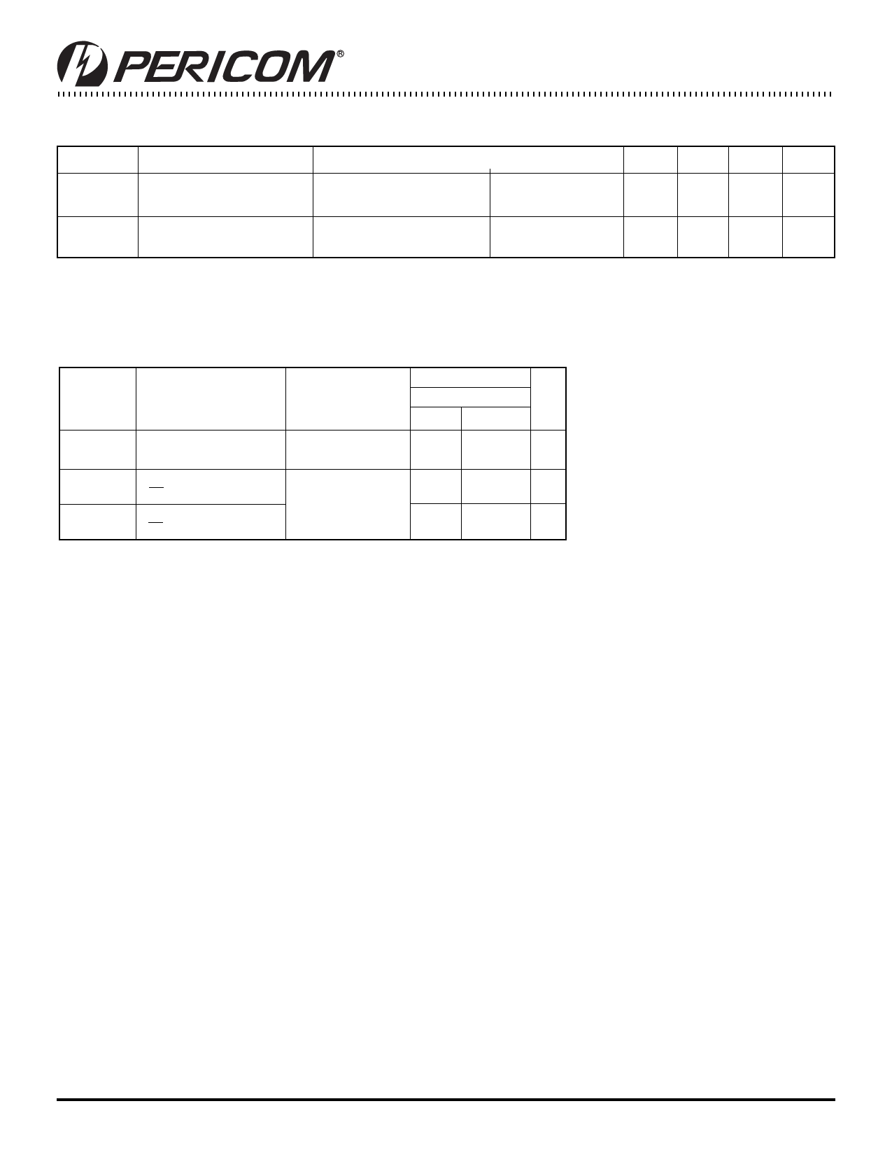
Power Supply Characteristics
Parameters Description
Test Conditions(1)
Min. Typ(2) Max.
ICC
Quiescent Power
Supply Current
VCC = Max.
VIN = GND or VCC
0.1 3.0
∆ICC
Supply Current per
VCC = Max.
VIN = 3.0V(3)
750
Input @ TTL HIGH
Notes:
1. For Max. or Min. conditions, use appropriate value specified under Electrical Characteristics for the applicable device.
2. Typical values are at VCC = 3.3V, +25°C ambient.
3. Per TTL driven input (control inputs only); A and B pins do not contribute to ICC.
Switching Characteristics over Operating Range
PI3B3244
Parameters Description
Conditions(1)
Com.
Min. Max. Units
tPLH
Propagation Delay(2,3) CL = 50 pF,
tPHL
Ax to Bx
RL = 500Ω
tPZH
Bus Enable Time
CL = 50 pF,
tPZL
BE to Ax or Bx
RL = 500Ω,
tPHZ
Bus Disable Time
RL = 500Ω
tPLZ
BE to Ax or Bx
0.25 ns
1.0
4.0
ns
1.0
4.5
ns
Notes:
1. See test circuit and waveforms.
2. This parameter is guaranteed but not tested on Propagation Delays.
3. The bus switch contributes no propagational delay other than the RC delay of the ON
resistance of the switch and the load capacitance. The time constant for the switch alone
is of the order of 0.25ns for 50pF load. Since this time constant is much smaller than the
rise/fall times of typical driving signals, it adds very little propagational delay to the
system. Propagational delay of the bus switch when used in a system is determined by
the driving circuit on the driving side of the switch and its interaction with the load on
the driven side.
Units
µA
µA
Applications Information
Logic Inputs
The logic control inputs can be driven up to +3.6 regardless of the supply voltage. For example, given a + 3.3V supply, IN may be
driven low to 0V and high to 3.6V. Driving IN Rail-to-Rail® minimizes power consumption.
Power-Supply Sequencing and Hot-Plug Information
Proper power-supply sequencing is recommended for all CMOS devices. Always apply VCC and GND before applying signals to
input/output or control pins.
Rail-to-Rail is a registeredtrademark of Nippon Motorola, Ltd
3
PS8149F 08/25/04
Share Link: 