PI3B33X257B 데이터 시트보기 (PDF) - Pericom Semiconductor
부품명
상세내역
일치하는 목록
PI3B33X257B Datasheet PDF : 4 Pages
| |||
PI3B33X257
3.3V, 24:12 Mux/DeMux NanoSwitch™
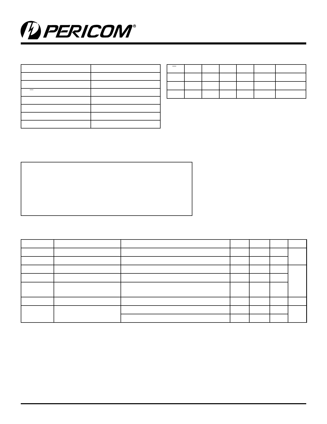
Pin Description
Pin Name
IAn-ILn
S
En
YA-YL
GND
VCC
NC
Description
Data Inputs
Select Inputs
Enable
Data Outputs
Ground
Power
No Connect
Truth Table(1)
En Sn YA(2) YB(2) YC(2)
H X Hi-Z Hi-Z Hi-Z
L
L
IA0 IB0 IC0
L
H
IA1 IB1 IC1
Notes:
1. H = High Voltage Level,
L = Low Voltage Level
2. n = 0 YA, YB, YC, YD,
n = 1 YE, YF, YG, YH,
n = 2 YI, YJ, YK, YL
YD(2)
Hi-Z
ID0
ID1
Function
Disable
S=0
S=1
Maximum Ratings
(Above which the useful life may be impaired. For user guidelines, not tested.)
Storage Temperature ............................................................ –65°C to +150°C
Ambient Temperature with Power Applied ........................... –40°C to +85°C
Supply Voltage to Ground Potential .......................................–0.5V to +4.6V
DC Input Voltage ....................................................................–0.5V to +4.6V
DC Output Current............................................................................... 120mA
Power Dissipation ................................................................................... 0.5W
Note:
Stresses greater than those listed under MAXIMUM RAT-
INGS may cause permanent damage to the device. This is
a stress rating only and functional operation of the device
at these or any other conditions above those indicated in
the operational sections of this specification is not implied.
Exposure to absolute maximum rating conditions for ex-
tended periods may affect reliability.
DC Electrical Characteristics (Over the Operating Range, TA = –40°C to +85°C, VCC = 3.3V ±5%)
Parameters Description
Test Conditions(1)
Min. Typ.(2)
VIH
Input HIGH Voltage
Guaranteed Logic HIGH Level
2.0
VIL
Input LOW Voltage
Guaranteed Logic LOW Level
–0.5
IIH
Input HIGH Current
VCC = Max., VIN = VCC
IIL
Input LOW Current
VCC = Max., VIN = GND
IOZH
High Impedance Output
Current
0 ≤ I, Y ≤ VCC
VIK
Clamp Diode Voltage
VCC = Min., IIN = –18mA
RON
Switch On-Resistance(3)
VCC = Min., VIN = 0.0V, ION = 48mA or 64mA
VCC = Min., VIN = 2.4V, ION = 15mA
5
10
Max.
0.8
±50
±1
±50
–1.2
7
15
Units
V
µA
V
Ω
2
PS8334D
11/01/04
Share Link: 