PI3B16292V 데이터 시트보기 (PDF) - Pericom Semiconductor
부품명
상세내역
일치하는 목록
PI3B16292V Datasheet PDF : 4 Pages
| |||
PI3B16292/162292
3.3V, 24-Bit Mux/Demux
BusSwitch (25Ω) 111222333444555666777888999000111222333444555666777888999000111222333444555666777888999000111222111222333444555666777888999000111222333444555666777888999000111222333444555666777888999000111222111222333444555666777888999000111222333444555666777888999000111222333444555666777888999000111222111222333444555666777888999000111222333444555666777888999000111222333444555666777888999000111222111222333444555666777888999000111222
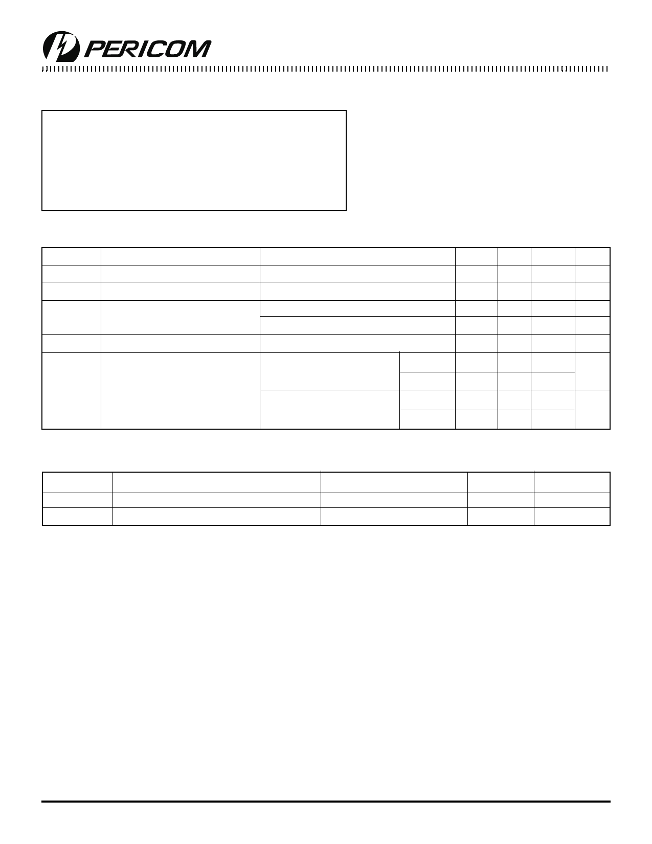
Maximum Ratings
(Above which the useful life may be impaired. For user guidelines, not tested.)
Storage Temperature ............................................ –65°C to +150°C
Ambient Temperature with Power Applied ............. –0°C to +85°C
Supply Voltage Range ............................................. –0.5V to +4.6V
DC Input Voltage .................................................... –0.5V to +4.6V
DC Output Current .............................................................. 120 mA
Power Dissipation ................................................................ 0.5Watt
Note:
Stresses greater than those listed under MAXIMUM
RATINGS may cause permanent damage to the device. This
is a stress rating only and functional operation of the device
at these or any other conditions above those indicated in the
operational sections of this specification is not implied.
Exposure to absolute maximum rating conditions for
extended periods may affect reliability.
DC Electrical Characteristics (Over the Operating Range, TA = –40°C to +85°C, VCC = 3.0V to 3.6V)
Parameters Description
VIH
Input HIGH Voltage
Test Conditions(1)
Guaranteed Logic HIGH Level
Min. Typ(2)
2.0 —
VIL
Input LOW Voltage
Guaranteed Logic LOW Level
–0.5 —
II
Input Current
VCC = Max., VIN = VCC or GND
VCC = 0, VIN = VCC
——
——
VIK
Clamp Diode Voltage
VCC = Min., IIN = –18mA
— –0.7
RON
Switch On Resistance(3)
VCC = Min., VIN = 0.0V,
16292 —
5
ION = 64mA
162292 20 28
VCC = Min., VIN = 2.4V,
16292 — 10
ION = 15mA
162292 20 35
Max.
—
0.8
±1
10
–1.2
8
40
15
48
Units
V
V
µA
µA
V
Ω
Ω
Capacitance (TA = 25°C, f = 1 MHz)
Parameters(4) Description
CIN
Input Capacitance
CON
A/B Capacitance, Switch On
Test Conditions
VIN = 0V
VIN = 0V
Max.
3.0
30.0
Units
pF
pF
Notes:
1. For Max. or Min. conditions, use appropriate value specified under Electrical Characteristics for the applicable device.
2. Typical values are at Vcc = 3.3V, TA = 25°C ambient and maximum loading.
3. Measured by the voltage drop between A and B pin at indicated current through the switch. ON resistance is determined by the
lower of the voltages on the two (A,B) pins.
4. This parameter is determined by device characterization but is not production tested.
2
PS8177A 12/14/98
Share Link: 