PI3B162292A 데이터 시트보기 (PDF) - Pericom Semiconductor
부품명
상세내역
일치하는 목록
PI3B162292A Datasheet PDF : 4 Pages
| |||
PI3B16292
PI3B162292 (25Ω) 1122334455667788990011223344556677889900112233445566778899001122112233445566778899001122334455667788990011223344556677889900112211223344556677889900112233445566778899001122334455667788990011221122334455667788990011223344556677889900112233445566778899001122112233445566778899001122
3.3Volt, 24-Bit
Features
Description
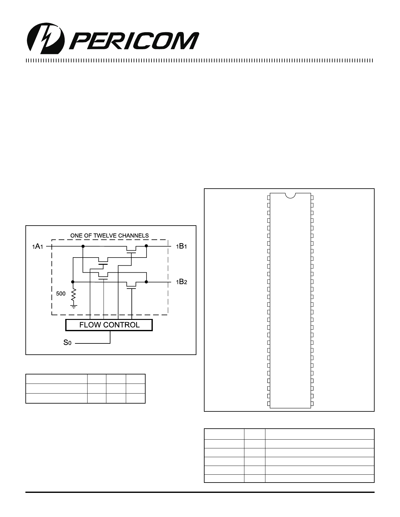
Mux/Demux BusSwitch
• Near-zero propagation delay
• 5Ω switches connect inputs to outputs
Pericom Semiconductor’s PI3B series of logic circuits are produced
using the Company’s advanced 0.35 micron CMOS technology.
• Fast Switching Speed - 5ns (max.)(16292)
• Internal 500Ω pull-down on A2 ports
• Ultra-low quiescent power (0.2µA typical) – Ideally
suited for notebook applications
• Vcc Operating Range : 3.0V to 3.6V
• Industrial operating temperature: –40°C to +85°C
• Make-before-break switching
• Packages available:
– 56-pin 240-mil wide thin plastic TSSOP (A)
– 56-pin 300-mil wide plastic SSOP (V)
The PI3B16292 and PI3B162292 are 3.3 volt, 12-bit to 24-bit
Mux/Demux Bus switches designed with a low ON resistance
allowing inputs to be connected directly to outputs.
The PI3B162292 device has a built-in 25-ohm series resistor
to reduce noise resulting from reflections, thus eliminating the
need for an external terminating resistor.
A2 port is not externally connected and, as a result, has an internal
500-ohm pulldown resistor to ground.
Pin Configuration
Applications
• Memory switching
S0 1
1A1 2
56 NC
55 NC
Logic Block Diagram
NC1 3
2A1 4
54 1B1
53 1B2
NC1 5
52 2B1
3A1 6
NC1 7
51 2B2
50 3B1
GND 8
49 GND
4A1 9
48 3B2
NC1 10
5A1 11
47 4B1
46 4B2
NC1 12 56-PIN 45 5B1
6A1 13 A, V 44 5B2
Ω
NC1 14
43 6B1
7A1 15
42 6B2
NC1 16
41 7B1
VCC 17
8A1 18
GND 19
40 7B2
39 8B1
38 GND
NC1 20
37 8B2
Truth Table
Function
S0
A1 to B1, A2 to B2 L
A1 A2
B1 B2
9A1 21
NC1 22
10A1 23
NC1 24
11A1 25
NC1 26
36 9B1
35 9B2
34 10B1
33 10B2
32 11B1
31 11B2
A1 to B2, A2 to B1 H
Note:
1. H = High Voltage Level
L = Low Voltage Level
Z = High Impedance
B2 B1
12A1 27
NC1 28
30 12B1
29 12B2
Product Pin Description
Pin Name I/O
Description
S0
I Select Inputs
xA1
I/O Bus A
xBx
I/O Bus B
NC
Leave it unconnected
NC1
Leave it unconnected
1
PS8177A 12/14/98
Share Link: 