PI3B162861 데이터 시트보기 (PDF) - Pericom Semiconductor
부품명
상세내역
일치하는 목록
PI3B162861 Datasheet PDF : 3 Pages
| |||
PI3B16861/PI3B162861
1234567890123456789012345678901212345678901234567890123456789012123456789012345367.839V012,3H456o7t89I0n12s1e2r34t5i6o7n89,0122034-5B67i8t9,0212-3P45o6r78t90B12u1s23S4w567i8t9c0h12
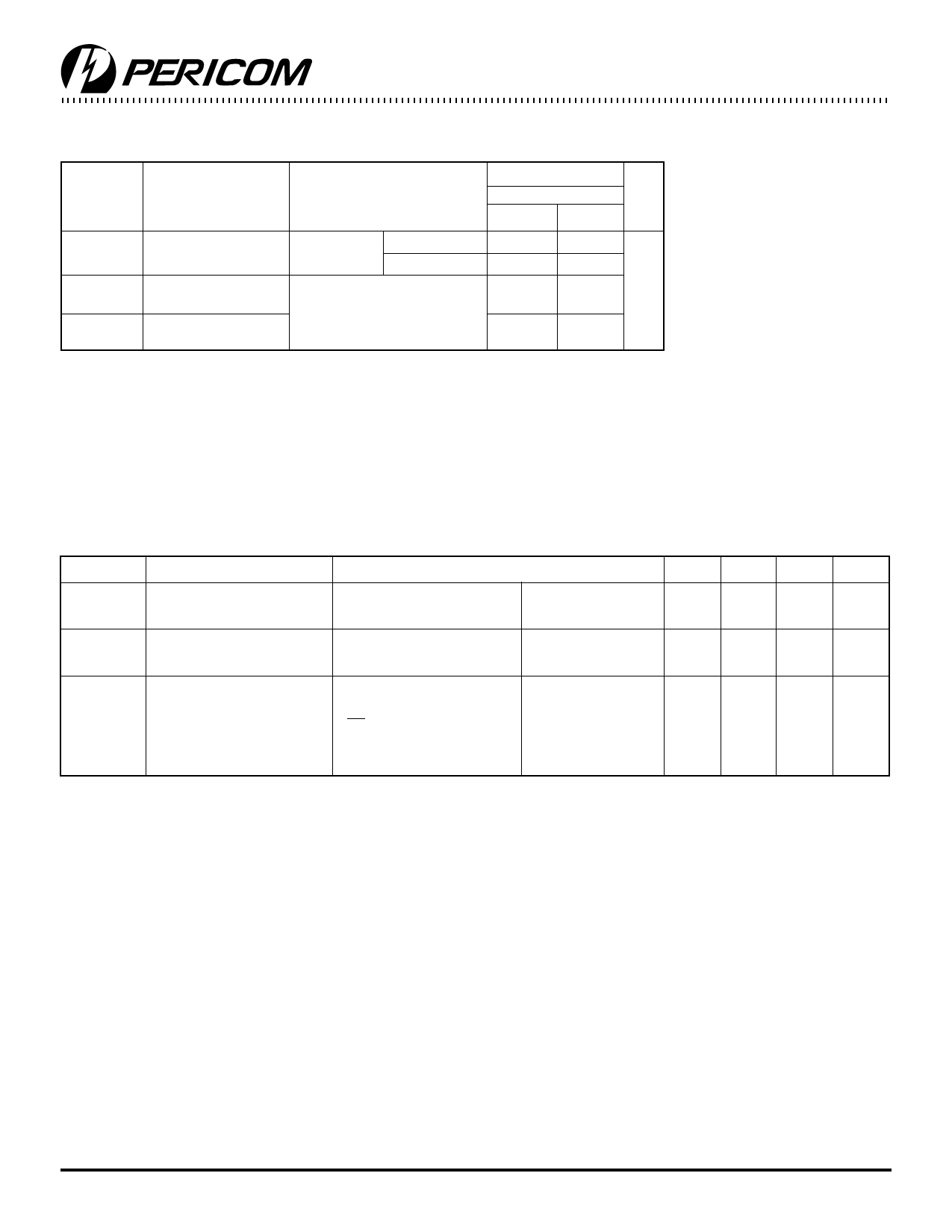
Switching Characteristics over Operating Range
Parameters Description
Conditions(1)
PI3B16861/PI3B162861
Com.
Min.
Max.
Units
tPLH
Propagation Delay(2,3) CL = 50pF
16861
tPHL
Ax to Bx, Bx to Ax
RL = 500Ω 162861
tPZH
Bus Enable Time
CL = 50pF,
tPZL
BE to Ax or Bx
RL = 500Ω,
tPHZ
Bus Disable Time
R = 500Ω
tPLZ
BE to Ax or Bx
—
0.25
—
1.25
1
4.5
ns
1
5
Notes:
1. See test circuit and waveforms.
2. This parameter is guaranteed but not tested on Propagation Delays.
3. The bus switch contributes no propagational delay other than the RC delay of the ON resistance of the switch and the load
capacitance. The time constant for the switch alone is of the order of 0.25ns for 50pF load. Since this time constant is much
smaller than the rise/fall times of typical driving signals, it adds very little propagational delay to the system. Propagational
delay of the bus switch when used in a system is determined by the driving circuit on the driving side of the switch and its
interaction with the load on the driven side.
Power Supply Characteristics
Parameters Description
ICC
Quiescent Power
Supply Current
∆ICC
Supply Current per
Input @ TTL HIGH
ICCD
Supply Current per
Input per MHz(4)
Test Conditions(1)
VCC = Max.
VIN = GND or VCC
Min. Typ(2) Max. Units
10 µA
VCC = Max.
VIN = 3.0V(3)
750 µA
VCC = Max.
A and B Pins Open
BE = GND
Control Input Toggling
50% Duty Cycle
0.25 mA/
MHz
Notes:
1. For Max. or Min. conditions, use appropriate value specified under Electrical Characteristics for the applicable device.
2. Typical values are at Vcc = 3.3V, +25°C ambient.
3. Per TTL driven input (control inputs only); A and B pins do not contribute to Icc.
4. This current applies to the control inputs only and represent the current required to switch internal capacitance at the
specified frequency. The A and B inputs generate no significant AC or DC currents as they transition. This parameter
is not tested, but is guaranteed by design.
Pericom Semiconductor Corporation
2380 Bering Drive • San Jose, CA 95131 • 1-800-435-2336 • Fax (408) 435-1100 • http://www.pericom.com
3
PS8175B 11/06/98
Share Link: 