PI3B16224B 데이터 시트보기 (PDF) - Pericom Semiconductor
부품명
상세내역
일치하는 목록
PI3B16224B Datasheet PDF : 3 Pages
| |||
PI3B16224
3.3V, 12-Bit to 24-Bit
DeMux/Mux NanoSwitch™
1122334455667788990011223344556677889900112233445566778899001122112233445566778899001122334455667788990011223344556677889900112211223344556677889900112233445566778899001122334455667788990011221122334455667788990011223344556677889900112233445566778899001122112233445566778899001122
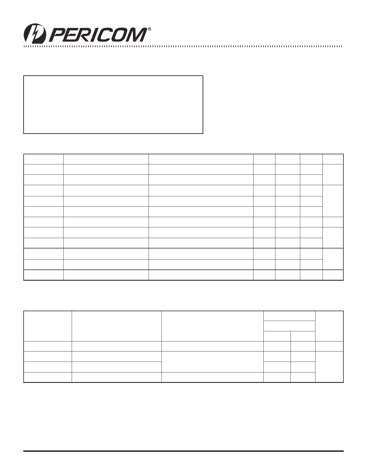
Maximum Ratings
(Above which useful life may be impaired. For user guidelines, not tested.)
Storage Temperature Range, TSTG ......................................... –65ºC to +150ºC
Ambient Temperature with Power Applied ..................... –40ºC to +85ºC
Supply Voltage Range, to Ground Potential .................... –0.5V to +4.6V
Input Voltage Range .......................................................... –0.5Vto+4.6V
DC Output Current ......................................................................... 120mA
Power Dissipation ............................................................................. 0.5W
Note:
Stresses greater than those listed under MAXIMUM
RATINGS may cause permanent damage to the device.
This is a stress rating only and functional operation of the
device at these or any other conditions above those
indicated in the operational sections of this specification
is not implied. Exposure to absolute maximum rating
conditions for extended periods may affect reliability.
DC Electrical Characteristics (Over the Operating Range, TA = –40ºC to +85ºC, VCC = 3.0 to 3.6V)
Parameters
Description
Test Conditions(1)
Min. Typ.(2) Max. Units
VIH
Input HIGH Voltage
Guaranteed Logic High Level
VIL
Input LOW Voltage
Guaranteed Logic Low Level
IIH
Input HIGH Current
VCC = Max.; VIN = VCC
IIL
Input LOW Current
VCC = Max.; VIN = GND
IOZH
High Impedance Output Current 0 ≤ A, B ≤ VCC
VIK
Clamp Diode Voltage
VCC = Min, IIN = –18mA
RON
Switch On Resistance
VCC = Min., VIN = 0.0V, ION = 12mA
RON
Switch On Resistance
VCC = Min., VIN = 2.4V, ION = 12mA
CIN
Input Capacitance
VIN = 0V, 25°C, f = 1 MHz
CON
A/B Capacitance
VIN = 0V, 25°C, f = 1 MHz
ICC
Power Supply Quiescent
Notes:
1. Typical values are shown at VCC = 3.3V, +25°C ambient and maximum loading.
2.0
V
–0.5
0.8
±1
±1 µA
±1
–0.7 –1.2 V
5
8
Ω
10
15
3.0
pF
25.0
10 µA
Switching Electrical Characteristics (TA = –40ºC to +85ºC, VCC = 3.0 to 3.6V)
PI3B16224
Com.
Parameters
tPLH
tPE
tPD
tM
Description
Propagation Delay Ax to xBx
Bus Enable
Bus Disable
Make-before-break time
Test Conditions
CL = 50pF, RL = 500 ohms(1,2,3)
CL = 50pF, RL = 500 ohms(3)
CL = 50pF, RL = 500 ohms(1)
Min.
–
1
1
0
Max.
250
4.5
5.0
2
Units
ps
ns
Notes:
1. This parameter is guaranteed but not tested on Propagation Delays.
2. The bus switch contributes no propagational delay other than the RC delay of the ON resistance of the switch and the load
capacitance. The time constant for the switch alone is of the order of 0.25ns for 50pF load. Since this time constant is much
smaller than the rise/fall times of typical driving signals, it adds very little propagational delay to the system. Propagational delay
of the bus switch when used in a system is determined by the driving circuit on the driving side of the switch and its interaction
with the load on the driven side.
3. See test circuit and waveforms.
2
PS8181E 09/10/04
Share Link: 