PI6C2305-1LI 데이터 시트보기 (PDF) - Pericom Semiconductor
부품명
상세내역
일치하는 목록
PI6C2305-1LI Datasheet PDF : 9 Pages
| |||
PI6C2305/PI6C2309
Zero Delay Clock Buffer 1122334455667788990011223344556677889900112233445566778899001122112233445566778899001122334455667788990011223344556677889900112211223344556677889900112233445566778899001122334455667788990011221122334455667788990011223344556677889900112233445566778899001122112233445566778899001122
Zero Delay and Skew Control
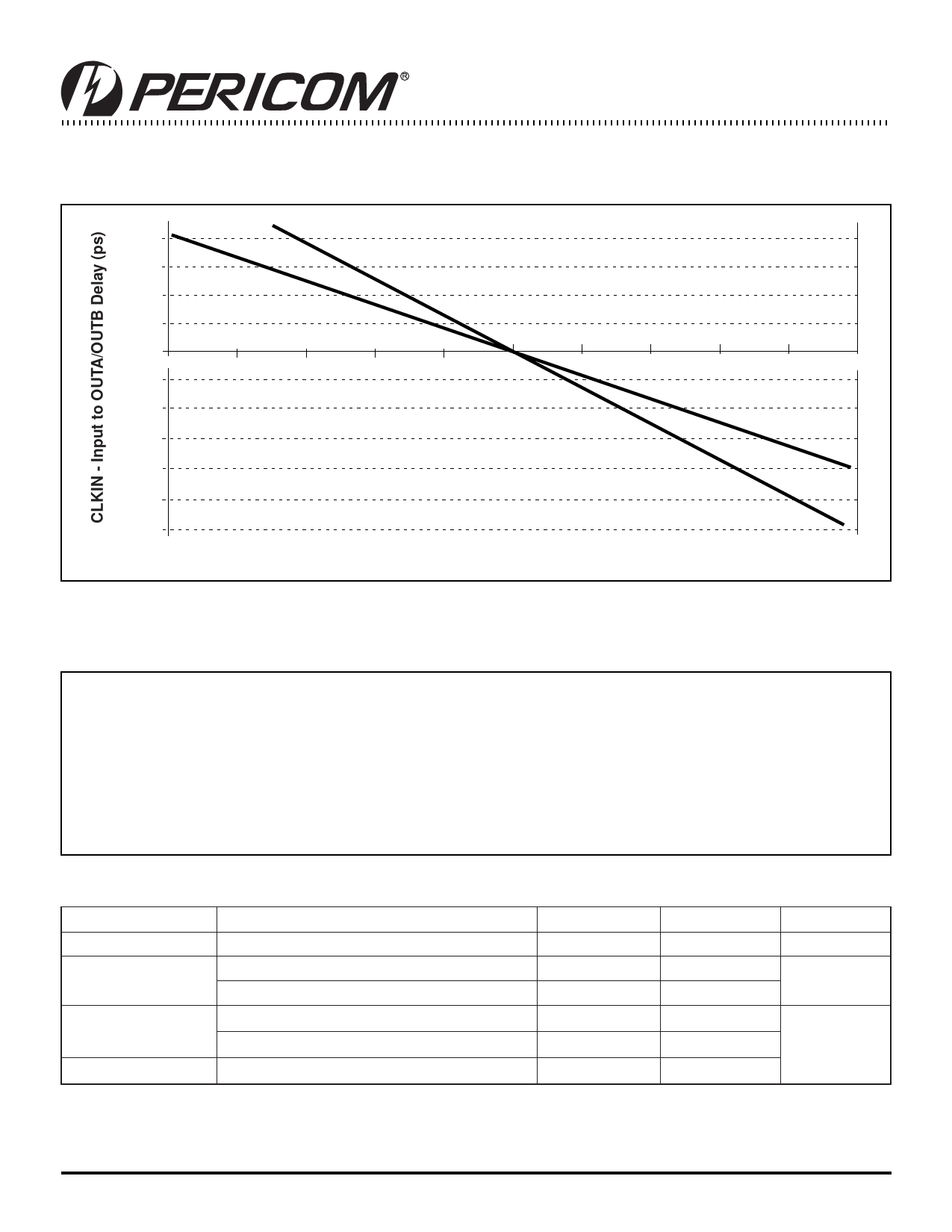
CLKIN Input to OUTA/OUTB Delay vs. Difference in Loading between OUT0 pin and OUTA/OUTB pins
800
600
400
200
0
-25
-20
-15
-10
-5
0
5
10
15
20
25
-200
-400
-600
PI6C2305-1H
PI6C2309-1H
-800
-900
-1000
PI6C2309-1
PI6C2305-1
Output Load Difference: OUT0 - OUTA/OUTB Load (pF)
The relationship between loading of the FB_IN signal and other outputs determines the input-output delay. Zero delay is achieved when
all outputs, including feedback, are loaded equally.
Maximum Ratings
Supply Voltage to Ground Potential ............................................................................................................................. 0.5Vto+7.0V
DC Input Voltage (Except CLKIN) ........................................................................................................................ 0.5VtoVDD+0.5V
DC Input Voltage CLKIN ...................................................................................................................................................... 0.5 to 7V
Storage Temperature ................................................................................................................................................... 65ºC to +150ºC
Maximum Soldering Temperature (10 seconds) ........................................................................................................................... 260ºC
Junction Temperature .................................................................................................................................................................. 150ºC
Static Discharge Voltage (per MIL-STD-883, Method 3015) .................................................................................................... >2000V
Operating Conditions (VCC = 3.3V ±0.3V)
Parameter
Description
Min.
VDD
Supply Voltage
3.0
Commerical Operating Temperature
0
TA
Industrial Operating Temperature
40
Load Capacitance, below 100 MHz
¾
CL
Load Capacitance, from 100 MHz to 133 MHz
¾
CIN
Input Capacitance
¾
Max.
3.6
70
85
30
15
7
Units
V
ºC
pF
3
PS8478B 10/30/01
Share Link: 