US1075CP 데이터 시트보기 (PDF) - Unisem
부품명
상세내역
일치하는 목록
US1075CP Datasheet PDF : 5 Pages
| |||
US1075
ABSOLUTE MAXIMUM RATINGS
Input Voltage (Vin) .................................................................. 7V
Power Dissipation ............................................ Internally Limited
Storage Temperature Range .............................. -65°C TO 150°C
Operating Junction Temperature Range .................. 0°C TO 150°C
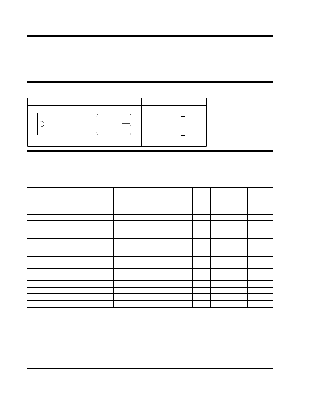
PACKAGE INFORMATION
3 PIN PLASTIC TO220 ( T ) 3 PIN PLASTIC TO263 ( M ) 3 PIN PLASTIC POWER FLEX ( P )
FRONT VIEW
3
Vin
Tab is
Vout
2
Vout
1
Adj
θJT=2.7°C/W θJA=60°C/W
FRONT VIEW
3
Vin
Tab is
Vout
2
Vout
1
Adj
θJA=35°C/W for 1" Square pad
FRONT VIEW
3
Vin
Tab is
Vout
2
Vout
1
Adj
θJA=35°C/W for 1" Square pad
ELECTRICAL SPECIFICATIONS
Unless otherwise specified ,these specifications apply over ,Cin=1uF,Cout=10uF,and Tj=0 to 150°C.Typical
values refer to Tj=25°C.
PARAMETER
Reference Voltage
Line Regulation
Load Regulation (note 1)
Dropout Voltage
(note 2)
Current Limit
Minimum Load Current
(note 3)
Thermal Regulation
Ripple Rejection
Adjust Pin Current
Adjust Pin Current Change
Temperature Stability
Long Term Stability
RMS Output Noise
SYM
VREF
∆VO
TEST CONDITION
Io=10mA,Tj=25°C,(Vin-Vo)=1.5V
Io=10mA, (Vin-Vo)=1.5V
Io=10mA,1.3V<(Vin-Vo)<7V
Vin=3.3V,Vadj=0,10mA<Io<7.5A
Io=7.5A
Io=4A
Vin=3.3V,dVo=100mV
Vin=3.3V,Vadj=0V
MIN
1.238
1.225
7.6
TYP
1.250
1.250
0.4
1.0
0.92
9
5
MAX
1.262
1.275
0.2
1.2
1.1
10
UNITS
V
%
%
V
A
mA
30 mS PULSE,Vin-Vo=3V,Io=7.5A
f=120HZ ,Co=25uF Tan
Io=7.5A,Vin-Vo=3V
60
IADJ Io=10mA,Vin-Vo=1.5V,Tj=25
Io=10mA,Vin-Vo=1.5V
Io=10mA,Vin-Vo=1.5V,Tj=25
Vin=3.3V,Vadj=0V,Io=10mA
Tj=125°C,1000 Hrs
Tj=25°C 10hz<f<10khz
0.02
70
55 120
0.2 5
0.5
0.3
0.003
%/W
dB
uA
uA
%
%
%Vo
Note 1 : Low duty cycle pulse testing with Kelvin con-
nections are required in order to maintain accurate data.
Note 2 : Drop-out voltage is defined as the minimum
differential voltage between Vin and Vout required to main-
tain regulation at Vout. It is measured when the output
voltage drops 1% below its nominal value.
Note 3 : Minimum load current is defined as the mini-
mum current required at the output in order for the out-
put voltage to maintain regulation. Typically the resistor
dividers are selected such that it automatically main-
tains this current.
2-34
Rev. 1.0
9/14/99
Share Link: 