BS616LV1015 데이터 시트보기 (PDF) - Brilliance Semiconductor
부품명
상세내역
일치하는 목록
BS616LV1015 Datasheet PDF : 9 Pages
| |||
BSI
BS616LV1015
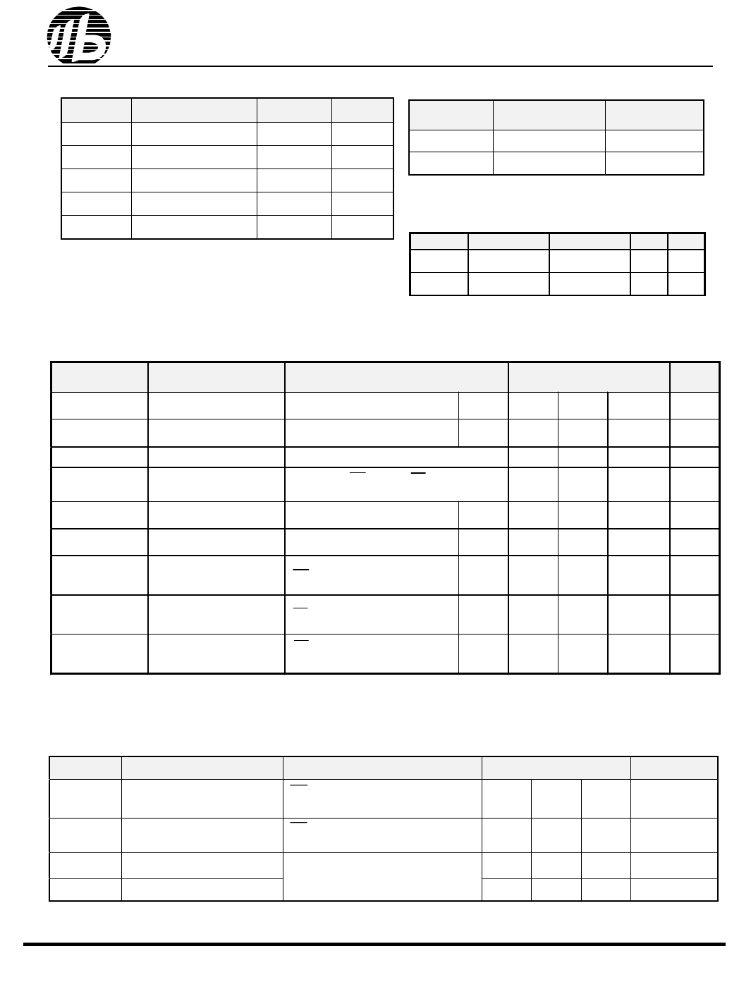
ABSOLUTE MAXIMUM RATINGS(1)
SYMBOL
VTERM
TBIAS
PARAMETER
Terminal Voltage with
Respect to GND
Temperature Under Bias
RATING
-0.5 to
Vcc+0.5
-40 to +85
TSTG
Storage Temperature
-60 to +150
UNITS
V
OC
OC
OPERATING RANGE
RANGE
Commercial
AMBIENT
TEMPERATURE
0 O C to +70 O C
Industrial
-40 O C to +85 O C
Vcc
4.5V ~ 5.5V
4.5V ~ 5.5V
PT
IOUT
Power Dissipation
DC Output Current
1.0
W
CAPACITANCE (1) (TA = 25oC, f = 1.0 MHz)
20
mA
SYMBOL PARAMETER CONDITIONS MAX. UNIT
1. Stresses greater than those listed under ABSOLUTE MAXIMUM
RATINGS may cause permanent damage to the device. This is a
stress rating only and functional operation of the device at these
or any other conditions above those indicated in the operational
CIN
CDQ
Input
Capacitance
Input/Output
Capacitance
VIN=0V
VI/O=0V
6
pF
8
pF
sections of this specification is not implied. Exposure to absolute 1. This parameter is guaranteed and not 100% tested.
maximum rating conditions for extended periods may affect
reliability.
DC ELECTRICAL CHARACTERISTICS ( TA = 0oC to + 70oC )
PARAMETER
NAME
VIL
VIH
PARAMETER
Guaranteed Input Low
Voltage(2)
Guaranteed Input High
Voltage(2)
TEST CONDITIONS
Vcc=5.0V
Vcc=5.0V
MIN. TYP. (1) MAX.
UNITS
-0.5
--
0.8
V
2.2
--
Vcc+0.2
V
IIL
Input Leakage Current Vcc = Max, VIN = 0V to Vcc
--
--
1
uA
ILO
Output Leakage Current
Vcc = Max, CE = VIH, or OE = VIH,
VI/O = 0V to Vcc
--
--
1
uA
VOL
Output Low Voltage
Vcc = Max, IOL = 2mA
Vcc=5.0V
--
--
0.4
V
VOH
Output High Voltage
Vcc = Min, IOH = -1mA
Vcc=5.0V
2.4
--
--
V
ICC
Operating Power Supply
Current
CE = VIL, IDQ = 0mA, F = Fmax(3)
Vcc=5.0V
--
--
35
mA
ICCSB
Standby Current-TTL
CE = VIH, IDQ = 0mA
Vcc=5.0V
--
--
2
mA
CE ≧ Vcc-0.2V,
ICCSB1
Standby Current-CMOS VIN ≧ Vcc - 0.2V or VIN ≦ 0.2V Vcc=5.0V
--
0.4
10
uA
1. Typical characteristics are at TA = 25oC.
2. These are absolute values with respect to device ground and all overshoots due to system or tester notice are included.
3. Fmax = 1/tRC .
DATA RETENTION CHARACTERISTICS ( TA = 0oC to + 70oC )
SYMBOL
PARAMETER
TEST CONDITIONS
MIN. TYP. (1) MAX.
UNITS
CE ≧ Vcc - 0.2V
VDR
Vcc for Data Retention
VIN ≧ Vcc - 0.2V or VIN ≦ 0.2V
1.5
--
--
V
ICCDR
Data Retention Current
CE ≧ Vcc - 0.2V
VIN ≧ Vcc - 0.2V or VIN ≦ 0.2V
--
0.02
0.3
uA
tCDR
Chip Deselect to Data
Retention Time
See Retention Waveform
tR
Operation Recovery Time
0
--
--
ns
TRC (2)
--
--
ns
1. Vcc = 1.5V, TA = + 25OC
2. tRC = Read Cycle Time
R0201-BS616LV1015
3
Revision 1.1
Jan. 2004
Share Link: 