BA6492 데이터 시트보기 (PDF) - ROHM Semiconductor
부품명
상세내역
일치하는 목록
BA6492 Datasheet PDF : 13 Pages
| |||
Motor driver ICs
BA6492BFS
FCircuit operation
(1) Motor drive circuits
The motor driver employs a 3-phase, full-wave soft
switching current drive system, in which the rotor position
is sensed by Hall elements. The motor drive current is
sensed by a small resistor (RNF). The total drive current
is controlled and limited by sensing the voltage devel-
oped across this resistor. The motor drive circuit consists
of Hall amplifiers, an amplitude control circuit, a driver, an
error amplifier, and a current feedback amplifier (Fig. 14).
The waveforms of different steps along the signal path
from the Hall elements to the motor driver output are
shown in Fig. 15. The Hall amplifiers receive the Hall ele-
ments voltage signals as differential inputs. Next, by de-
ducting the voltage signal of Hall elements 2 from the
voltage signal of Hall elements 1, current signal H1,
which has a phase 30 degrees ahead of Hall elements 1,
is created. Current signals H2 and H3 are created like-
wise. The amplitude control circuit then amplifies the H1,
H2, and H3 signals according to the current feedback
amplifier signal. Then, drive current signals are produced
at A1, A2, and A3 by applying a constant magnification
factor. Because a soft switching system is employed, the
drive current has low noise and a low total current ripple.
The total drive current is controlled by the error amplifier
input voltage. The error amplifier has a voltage gain of
about –11dB (a factor of 0.28). The current feedback am-
plifier regulates the total drive current, so that the error
amplifier output voltage (V1) becomes equal to the VRNF
voltage, which has been voltage-converted from the total
drive current through the RNF pin. If V1 exceeds the cur-
rent limiter voltage (Vcl), the constant voltage Vcl takes
precedence, and a current limit is provided at the level of
Vcl / RNF.
The current feedback amplifier tends to oscillate be-
cause it receives all the feedback with a gain of 0dB. To
prevent this oscillation, connect an external capacitor to
the CNF pin for phase compensation and for reducing the
high frequency gain.
(2) Speed control circuit
The speed control circuit is a non-adjustable digital servo
system that uses a frequency locked loop (FLL). The cir-
cuit consists of an 1 / 2 frequency divider, an FG amplifier,
and a speed discriminator (Fig. 16).
An internal reference clock is generated from an external
clock signal input. The 1 / 2 frequency divider reduces the
frequency of the OSC signal. The FG amplifier amplifies
the minute voltage generated by the motor FG pattern
and produces a rectangular-shaped speed signal. The
FG amplifier gain (GFG = 42dB, typical) is determined by
the internal resistance ratio.
For noise filtering, a high-pass filter is given by C3 and a
resistor of 1.6kΩ (typical), and a low-pass filter is given
by C4 and a resistor of 200kΩ (typical). The cutoff fre-
quencies of high-pass and low-pass filters (fH and fL, re-
spectively) are given by:
fH=
1
fL=
1
2π 1.6kΩ C3
2π 200kΩ C4
The C3 and C4 capacitances should be set so as to satis-
fy the following relationship:
fHtfFGtfL
where fFG is the FG frequency. Note that the FG amplifier
inputs have a hysteresis.
The speed discriminator divides the reference clock and
compares it with the reference frequency, and then out-
puts an error pulse according to the frequency difference.
The motor rotational speed N is given by:
N=60 S
fosc
S
1
(1)
n
z
fosc is the reference clock frequency,
n is (speed discriminator count) 2,
z is the FG tooth number.
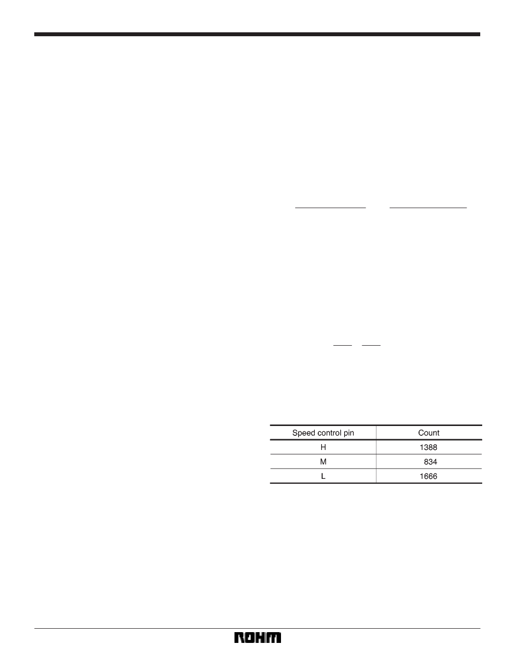
The discriminator count depends on the speed control
pin voltage.
The integrator flattens out the error pulse of the speed
discriminator and creates a control signal for the motor
drive circuit (Fig. 17).
561
Share Link: 