AK9822 데이터 시트보기 (PDF) - Asahi Kasei Microdevices
부품명
상세내역
일치하는 목록
AK9822 Datasheet PDF : 17 Pages
| |||
ASAHI KASEI
[AK9822/24]
Output of D/A converter
The output of the D/A converters can be set by the WRITE and the CALL instructions.
Upper 8bit data (D15∼D8) of the first address of the internal EEPROM (the address "0")
corresponds to "AO" of the D/A converter output. Lower 8bit data (D7∼D0) of the address "0"
corresponds to "A1". The internal composition of EEPROM is shown in the table2.
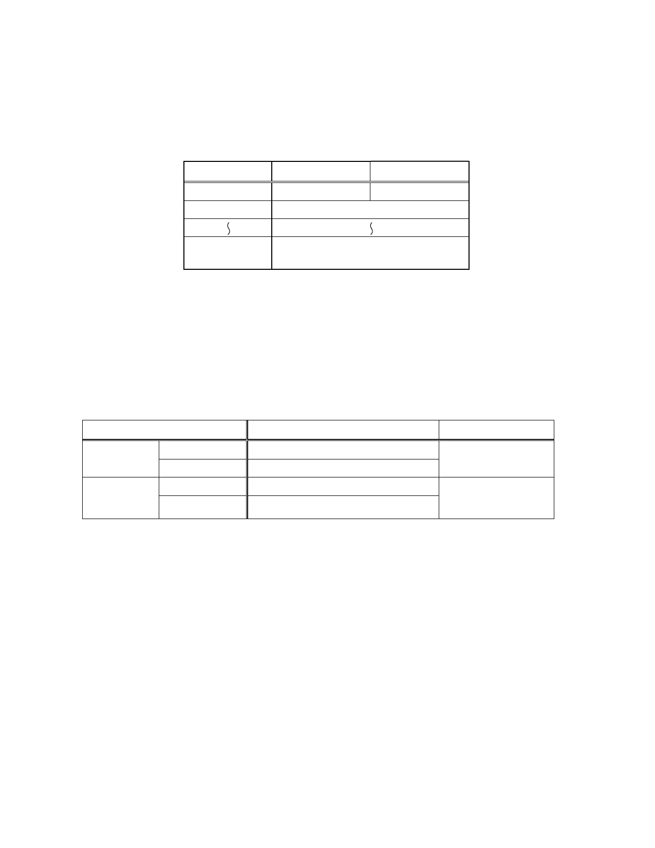
Address
0
1
D15∼D8
D7∼D0
Set data of A0 Set data of A1
General purpose memory
127(AK9822)
/255(AK9824)
General purpose memory
Table2. Internal composition of EEPROM
If the WRITE instruction by which the address "0" is specified is executed at the normal mode, the
outputs of the D/A converter of A0 and A1 are set by the specified data.
When the WRITE instruction by which the address "0" is specified is executed at the WRITE enable
state and the normal mode, the data is written in the address "0" of EEPROM and the outputs of the
D/A converter are set. When the WRITE instruction by which the address "0" is specified is
executed at the WRITE disable state and the normal mode, the data is not written in EEPROM and
the outputs of the D/A converter are set. Table3 shows the relation between EEPROM, D/A
converter and WRITE instruction.
State of AK9822/24
State of address"0"
Output of A0 and A1
Power down
mode
WRITE enable The data change to the specified data.
WRITE disable The data does not change.
The DAC outputs
are "Hi-Z".
Normal mode
WRITE enable The data change to the specified data.
WRITE disable The data does not change.
The DAC outputs
change to the
specified data.
Table3. Relation between EEPROM, D/A converter and WRITE instruction
If the CALL instruction is executed, the outputs of the D/A converter are set by the data of the
general purpose memory (AK9822:address "1" -"127", AK9824:address "1" -"255"). The CALL
instruction is composed by the op-code and the address.
When the CALL instruction is executed at the normal mode, the D/A converter output of A0 is set by
the upper 8bit data (D15∼D8) of the specified address and the output of A1 is set by the lower 8bit
data (D7∼D0). The CALL instruction is not executed at the power down mode.
DAD01E-00
-4-
1999/05
Share Link: 