CY7C143-35JI 데이터 시트보기 (PDF) - Cypress Semiconductor
부품명
상세내역
일치하는 목록
CY7C143-35JI Datasheet PDF : 13 Pages
| |||
Switching Waveforms (continued)
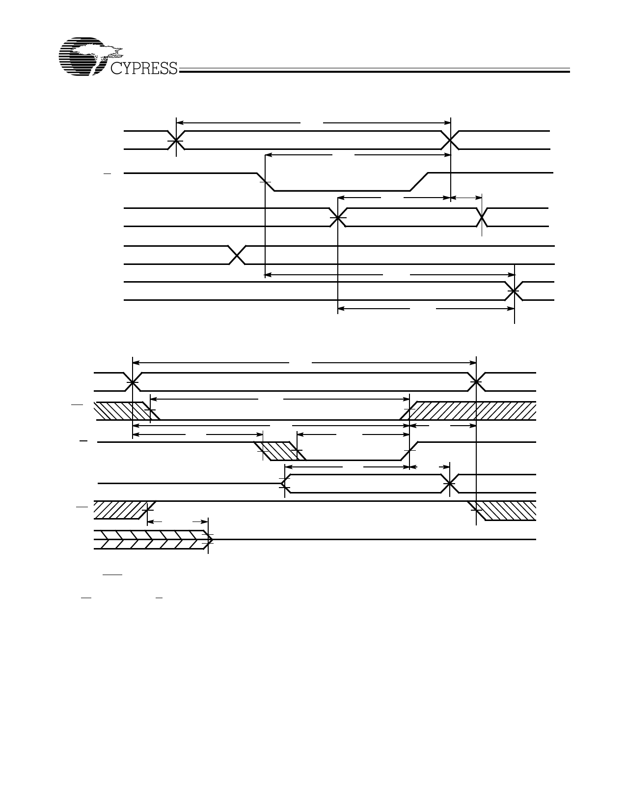
Timing Waveform of Read with Port-to-port Delay No. 4 (for slave CY7C143) [24, 25, 26]
ADDRESSR
tWC
MATCH
tWP
R/WR
DINR
tDW
VALID
CY7C133
CY7C143
tDH
ADDRESSL
DOUTL
MATCH
tWDD
tDDD
Write Cycle No. 1 (OE Three-States Data I/Os - Either Port) [17, 27]
Either Port
tWC
ADDRESS
CE
R/W
tSCE
tAW
tHA
tSA
tPWE
DATAIN
tSD
tHD
DATA VALID
VALID
OE
DOUT
tHZOE
HIGH IMPEDANCE
Notes:
24. Assume BUSY input at VIH for the writing port and at VIL for the reading port.l
25. Write cycle parameters should be adhered to in order to ensure proper writing.
26. Device is continuously enabled for both ports.
27. If OE is LOW during a R/W controlled write cycle, the write pulse width must be the larger of tPWE or tHZWE + tSD to allow the data I/O pins to enter high
impedance and for data to be placed on the bus for the required tSD.
Document #: 38-06036 Rev. *B
Page 9 of 13
Share Link: 