AP5004(2010) 데이터 시트보기 (PDF) - Diodes Incorporated.
부품명
상세내역
일치하는 목록
AP5004 Datasheet PDF : 11 Pages
| |||
AP5004
PWM CONTROL 2.5A STEP-DOWN CONVERTER
Functional Description (Continued)
Output Capacitor Selection
An output capacitor is required to maintain the DC output voltage. Low ESR capacitors are preferred to keep the
output voltage ripple low. The characteristics of the output capacitor also affect the stability of the regulation
control system. The ESR dominates the impedance at the switching frequency.The output ripple is calculated as:
VRIPPLE ≅ ΔI× RESR
Output Rectifier Diode
The output rectifier diode supplies the current to the inductor when the high-side switch is OFF. To reduce losses
due to the diode forward voltage and recovery times, use a Schottky rectifier.
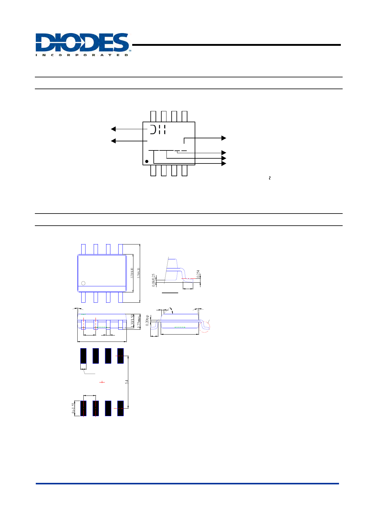
PCB Layout Guide
The dual Output pin (4) and VSS pins (7 & 8) on the SOP-8L package are internally connected to die pad. If low
TC & TJ or a large PD (Power Dissipation) is needed, the PCB layout should allow for maximum possible copper
area exposure at the SW pins. Please also follow the steps below to reduce switching noise.
1. Connect C3 to VCC and VSS pin as closely as possible to get good power filter effect.
2. Connect ground side of the C2 & D1 as closely as possible.
Typical PC Board Layout:
Top Side Layout Guide
Bottom Side Layout Guide
AP5004
Document number: DS31444 Rev. 5 - 2
9 of 11
www.diodes.com
August 2010
© Diodes Incorporated
Share Link: 