AMS1505CMV 데이터 시트보기 (PDF) - Advanced Monolithic Systems Inc
부품명
상세내역
일치하는 목록
AMS1505CMV Datasheet PDF : 8 Pages
| |||
AMS1505V
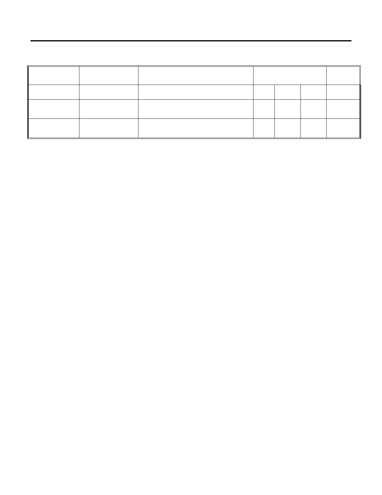
ELECTRICAL CHARACTERISTICS
Electrical Characteristics at IOUT = 0 mA, and TJ = +25°C unless otherwise specified.
Parameter
Device
Conditions
Min Typ Max Units
Dropout Voltage
Note 2
Control Dropout
(VCONTROL - VOUT)
Power Dropout
(VPOWER - VOUT)
AMS1505V/-1.5/-2.5/
-2.85/-3.0/-3.3/-3.5/-5.0
AMS1505V/-1.5/-2.5/
-2.85/-3.0/-3.3/-3.5/-5.0
VPOWER =VOUT + 0.8V, ILOAD = 10mA
VPOWER =VOUT + 0.8V, ILOAD = 5A
VCONTROL =VOUT + 2.5V, ILOAD = 3A
VCONTROL =VOUT + 2.5V, ILOAD = 5A
1.00
1.20
V
1.15
1.30
V
175
200
mV
300
350
mV
Parameters identified with boldface type apply over the full operating temperature range.
Note 1: Absolute Maximum Ratings indicate limits beyond which damage to the device may occur. For guaranteed specifications and test conditions, see the
Electrical Characteristics. The guaranteed specifications apply only for the test conditions listed.
Note 2: Unless otherwise specified VOUT = VSENSE. For the adjustable device VADJ = 0V.
Note 3: The dropout voltage for the AMS1505V is caused by either minimum control voltage or minimum power voltage. The specifications represent the
minimum input/output voltage required to maintain within 1% regulation.
Note 4: For the adjustable device the minimum load current is the minimum current required to maintain regulation. Normally the current in the resistor divider
used to set the output voltage is selected to meet the minimum load current requirement.
Note 5: The control pin current is the drive current required for the output transistor. This current will track output current with a ratio of about 1:100. The
minimum value is equal to the quiescent current of the device.
PIN FUNCTIONS
Sense (Pin 1): This pin is the positive side of the
reference voltage for the device. With this pin it is
possible to Kelvin sense the output voltage at the load.
Adjust/Ground (Pin 2): This pin is the negative side of
the reference voltage for the device. Adding a small
bypass capacitor from the Adjust pin to ground improves
the transient response.
Output (Pin 3): This is the power output of the device.
VCONTROL (Pin 4): This pin is the supply pin for the
control circuitry of the device. The current flow into
this pin will be about 1% of the output current. The
voltage at this pin must be 1.3V or greater than the
output voltage for the device to regulate.
VPOWER (Pin 5): This pin is the collector to the power
device of the AMS1505V. The output load current is
supplied through this pin. The voltage at this pin must
be between 0.1V and 0.35V greater than the output
voltage for the device to regulate.
Advanced Monolithic Systems, Inc. 6680B Sierra Lane, Dublin, CA 94568 Phone (925) 556-9090 Fax (925) 556-9140
Share Link: 