AK4589 데이터 시트보기 (PDF) - Asahi Kasei Microdevices
부품명
상세내역
일치하는 목록
AK4589 Datasheet PDF : 76 Pages
| |||
ASAHI KASEI
[AK4589]
Master mode and Slave mode
Master Mode can be selected by setting MASTER pin to “H”. LRCK1 and BICK1 will be outputs in Master Mode.
And, Slave Mode can be selected by setting this pin to “L”. LRCK1 and BICK1 will be inputs in Slave Mode.
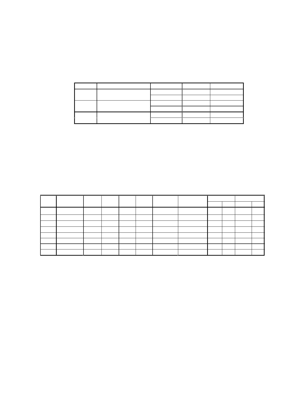
Operation of LRCK1 and BICK1 is shown below Table 9.
PDN pin
L
H
H
PWADN bit, PWDAN bit MASTER pin LRCK1 pin
--
L
Input
H
“L” output
“00”
L
Input
H
“L” output
Except for “00”
L
Input
H
Output
Table 9. Operation of LRCK1 and BICK1
BICK1 pin
Input
“L” output
Input
“L” output
Input
Output
Audio Serial Interface Format
When TDM1-0 bit = “00”, 8 modes can be selected by the DIF1-0 bits as shown in Table 10. In all modes the serial
data is MSB-first, 2’s complement format. The SDTO1 is clocked out on the falling edge of BICK1 and the
SDTI/DAUX1 are latched on the rising edge of BICK1. Figures 1∼4 shows the timing at SDOS bit = “0”. In this case,
the SDTO1 outputs the ADC output data. When SDOS bits = “1”, the data input to DAUX1 is converted to SDTO1’s
format and output from SDTO1. Mode 2, 3, 6, 7, 10, 11, 14, 15, 18, 19, 22, 23 in SDTI input formats can be used for
16-20bit data by zeroing the unused LSBs. In Table 10, Mode 2 is default setting. And M J shows MSB justified, L J
means LSB justified.
Mode
0
1
2
3
4
5
6
7
MASTER TDM1 TDM0 DIF1 DIF0 SDTO1
SDTI1-4,
DAUX1
LRCK1
I/O
BICK1
I/O
0
0
0
0
0 24bit, M J 20bit, L J H/L I ≥ 48fs I
0
0
0
0
1 24bit, M J 24bit, L J H/L I ≥ 48fs I
0
0
0
1
0 24bit, M J 24bit, M J H/L I ≥ 48fs I
0
0
0
1
1 24bit, I2S 24bit, I2S L/H I ≥ 48fs I
1
0
0
0
0 24bit, M J 20bit, L J H/L O 64fs O
1
0
0
0
1 24bit, M J 24bit, L J H/L O 64fs O
1
0
0
1
0 24bit, M J 24bit, M J H/L O 64fs O
1
0
0
1
1 24bit, I2S 24bit, I2S L/H O 64fs O
Table 10. Audio data formats (Normal mode, M J shows MSB justified, L J means LSB justified.)
The audio serial interface format becomes the TDM 256 mode if TDM1-0 bits are set to “01”. In the TDM 256 Mode,
the serial data of all DAC (eight channels) is input to the SDTI1 pin. The input data to SDTI2-4 pins is ignored. BICK1
should be fixed to 256fs. “H” time and “L” time of LRCK1 pin should be 1/256fs at least. Eight modes can be selected
by the DIF1-0 bits was shown in Table 11. In all modes the serial data is MSB-first, 2’s complement format. The
SDTO1 pin is clocked out on the falling edge of BICK1 pin and the SDTI1 pin are latched on the rising edge of BICK1
pin. SDOS bit and LOOP1-0 bits should be set to “0” in the TDM mode. TDM 128 Mode can be set by TDM1-0 bit =
“10”. In this Mode, the serial data of DAC (four channels; L1, R1, L2, R2) is input to the SDTI1 pin. Other four data
(L3, R3, L4, R4) are input to the SDTI2 pin.
MS0339-E-00
- 27 -
2004/09
Share Link: 