AK4588 데이터 시트보기 (PDF) - Asahi Kasei Microdevices
부품명
상세내역
일치하는 목록
AK4588 Datasheet PDF : 76 Pages
| |||
ASAHI KASEI
[AK4588]
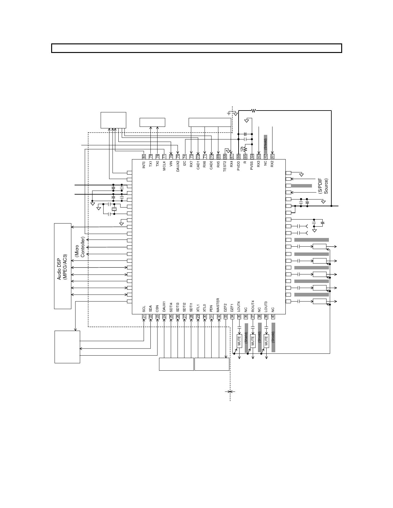
SYSTEM DESIGN
Figure 50 shows the system connection diagram. An evaluation board is available which demonstrates application
circuits, the optimum layout, power supply arrangements and measurement results.
Condition: I2C serial control mode
Audio DSP
(MPEG/AC3)
Micro
Controller
S/PDIF out
S/PDIF sources
5
10u
+
0.1u
(S/PDIF
sources)
3.3V to 5V
Digital
Digital 5V
1 INT1
2 BOUT
10u 0.1u
+
3 TVDD
4 DVDD
+
5 DVSS
C
6 XTO
X’tal
7 XTI
C
8 TEST3
9 MCKO2
10 MCKO1
11 COUT
12 UOUT
13 VOUT
14 SDTO2
15 BICK2
16 LRCK2
17 SDTO1
18 BICK1
19 LRCK1
20 CDTO
AK4588
TEST1 60
RX1 59
NC 58
RX0 57
AVSS 56
AVDD 55
VREFH 54
VCOM 53
RIN 52
LIN 51
NC 50
ROUT1 49
NC 48
LOUT1 47
NC 46
ROUT2 45
NC 44
LOUT2 43
NC 42
ROUT3 41
(Shield)
+
0.1u 10u Analog 5V
0.1u 2.2u
+
(Shield)
MUTE
(Shield)
MUTE
(Shield)
MUTE
(Shield)
MUTE
(Shield)
MUTE
Micro
Controller
Audio DSP
(MPEG/AC3)
Micro Controller
Digital Ground
Analog Ground
Figure 50. Typical Connection Diagram
Notes:
- “C” depends on the crystal.
- AVSS, DVSS and PVSS must be connected the same analog ground plane.
- Digital signals, especially clocks, should be kept away from the R pin in order to avoid an effect to the clock jitter
performance.
- In case of coaxial input, ground of RCA connector and terminator should be connected to PVSS of the AK4588
with low impedance on PC board.
MS0287-E-01
- 72 -
2004/03
Share Link: 