AK4586VQ 데이터 시트보기 (PDF) - Asahi Kasei Microdevices
부품명
상세내역
일치하는 목록
AK4586VQ Datasheet PDF : 54 Pages
| |||
ASAHI KASEI
[AK4586]
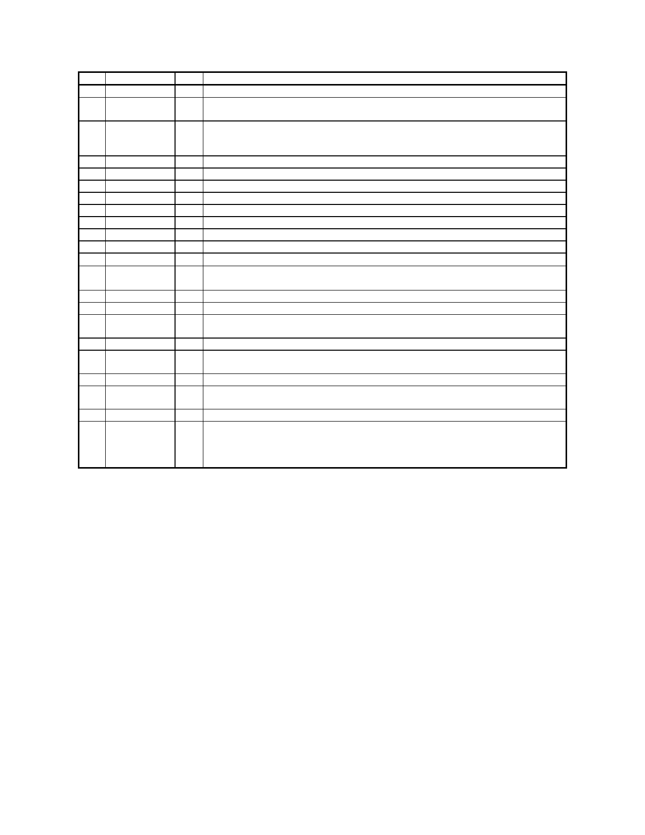
No. Pin Name
23 VREFH
24 VCOM
25 DZF1
26 LOUT3
27 ROUT3
28 LOUT2
29 ROUT2
30 LOUT1
31 ROUT1
32 LIN
33 RIN
34 PVDD
35 R
36 PVSS
37 RX4
38 SLAVE
39 RX3
40 TST
41 RX2
42 I2C
43 RX1
44 PDN
I/O
Function
I Positive Voltage Reference Input Pin, AVDD
O Common Voltage Output Pin, AVDD/2
Large external capacitor around 2.2µF is used to reduce power-supply noise.
O Zero Input Detect 1 Pin
(Note 1)
When the input data of the group 1 follow total 8192 LRCK cycles with “0” input data,
this pin goes to “H”.
O DAC3 Lch Analog Output Pin
O DAC3 Rch Analog Output Pin
O DAC2 Lch Analog Output Pin
O DAC2 Rch Analog Output Pin
O DAC1 Lch Analog Output Pin
O DAC1 Rch Analog Output Pin
I Lch Analog Input Pin
I Rch Analog Input Pin
- PLL Power Supply Pin, 4.5V∼5.5V
- External Resistor Pin
18kΩ +/-1% resistor to PVSS externally.
- PLL Ground Pin, 0V
I Receiver Channel 4 Pin (Internal biased pin)
I Slave Mode Pin
“L”: Master mode or Slave mode, “H”: Slave mode
I Receiver Channel 3 Pin (Internal biased pin)
I Test Pin
This pin should be connected to DVSS.
I Receiver Channel 2 Pin (Internal biased pin)
I Control Mode Select Pin
“L”: 4-wire Serial, “H”: I2C Bus
I Receiver Channel 1 Pin (Internal biased pin)
I Power-Down & Reset Pin
When “L”, the AK4586 is powered-down, all output pins go to “L” and the control
registers are reset to default state. If the state of CAD1-0 changes, then the AK4586
must be reset by PDN.
Notes:
1. The group 1 and 2 can be selected by DZFM2-0 bits.
2. This pin becomes OVF pin if OVFE bit is set to “1”.
3. All input pins except internal biased pins should not be left floating.
MS0097-E-01
-6-
2001/12
Share Link: 