AIC1653 데이터 시트보기 (PDF) - Analog Intergrations
부품명
상세내역
일치하는 목록
AIC1653 Datasheet PDF : 11 Pages
| |||
AIC1653
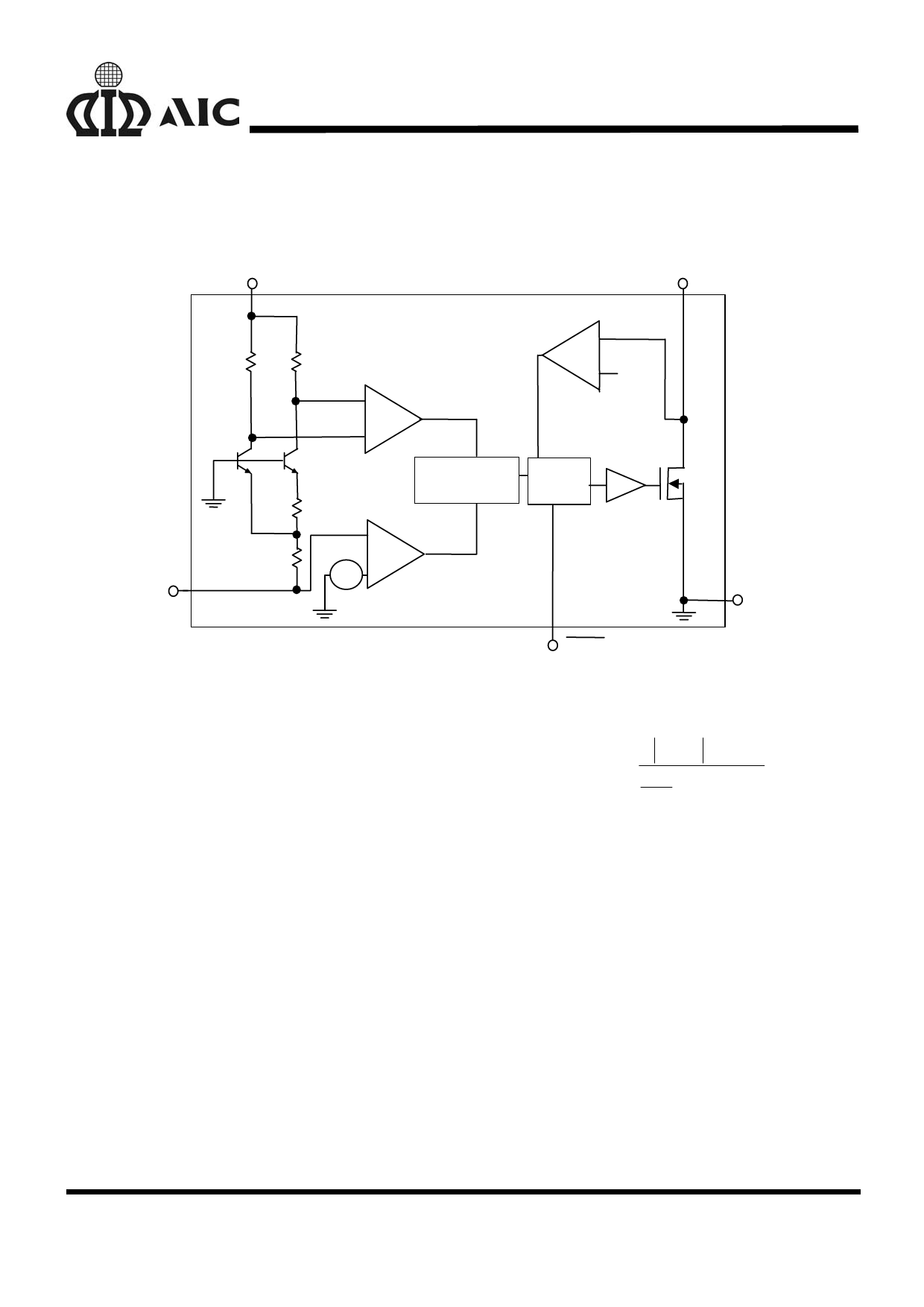
BLOCK DIAGRAM
VIN
SW
NFB
R1 R2
Q1
+ Bandgap
A1
-
+
A2
-
100mV
Current Limit
Q2
400nS/ 800nS Logic
One-Shot
R3
+
Drive
R4
A3
-+ -
MODE Control
-0.6V
SHDN
Fig. 8 Block diagram of AIC1653
GND
PIN DESCRIPTIONS
PIN 1: SW - Switch Pin. This is the open drain
of the internal N-MOSFET power
switch. Minimize the metal trace
area connected to this pin to
minimize EMI.
PIN 2: GND - Ground. Tie this pin directly to the
local ground plane.
PIN 3: FB - Set the output voltage by values
of R1 and R2 (see typical
application circuit):
R1 = VOUT − 1.23
1.23
R2
+
2 × 10 −6
PIN 4: SHDN - Shutdown Pin. Tie this pin to
0.9V or higher to enable the
device. Tie below 0.25V to turn
off the device.
PIN 5: VIN - Input Supply Pin. Bypass this pin
with a capacitor as close to the
device as possible.
6
Share Link: 