ADSP-21365(RevA) 데이터 시트보기 (PDF) - Analog Devices
부품명
상세내역
일치하는 목록
ADSP-21365 Datasheet PDF : 52 Pages
| |||
ADSP-21362/ADSP-21363/ADSP-21364/ADSP-21365/ADSP-21366
Harvard architecture, allow unconstrained data flow between
computation units and internal memory. The registers in PEX
are referred to as R0–R15 and in PEY as S0–S15.
Single-Cycle Fetch of Instruction and Four Operands
The ADSP-2136x features an enhanced Harvard architecture in
which the data memory (DM) bus transfers data and the pro-
gram memory (PM) bus transfers both instructions and data
(see Figure 1 on Page 1). With the processor’s separate program
and data memory buses and on-chip instruction cache, the pro-
cessor can simultaneously fetch four operands (two over each
data bus) and one instruction (from the cache), all in a
single cycle.
Instruction Cache
The ADSP-2136x includes an on-chip instruction cache that
enables three-bus operation for fetching an instruction and four
data values. The cache is selective—only the instructions whose
fetches conflict with PM bus data accesses are cached. This
cache allows full-speed execution of core, looped operations
such as digital filter multiply-accumulates, and FFT butterfly
processing.
Data Address Generators with Zero-Overhead Hardware
Circular Buffer Support
The ADSP-2136x’s two data address generators (DAGs) are
used for indirect addressing and implementing circular data
buffers in hardware. Circular buffers allow efficient program-
ming of delay lines and other data structures required in digital
signal processing, and are commonly used in digital filters and
Fourier transforms. The two DAGs contain sufficient registers
to allow the creation of up to 32 circular buffers (16 primary
register sets, 16 secondary). The DAGs automatically handle
address pointer wraparound, reduce overhead, increase perfor-
mance, and simplify implementation. Circular buffers can start
and end at any memory location.
Flexible Instruction Set
The 48-bit instruction word accommodates a variety of parallel
operations, for concise programming. For example, the
ADSP-2136x can conditionally execute a multiply, an add, and a
subtract in both processing elements while branching and fetch-
ing up to four 32-bit values from memory—all in a single
instruction.
MEMORY AND I/O INTERFACE FEATURES
The ADSP-2136x adds the following architectural features to
the SIMD SHARC family core.
On-Chip Memory
The ADSP-2136x contains three megabits of internal SRAM
and four megabits of internal ROM. Each block can be config-
ured for different combinations of code and data storage (see
Table 3). Each memory block supports single-cycle, indepen-
dent accesses by the core processor and I/O processor. The
processor’s memory architecture, in combination with its sepa-
rate on-chip buses, allows two data transfers from the core and
one from the I/O processor, in a single cycle.
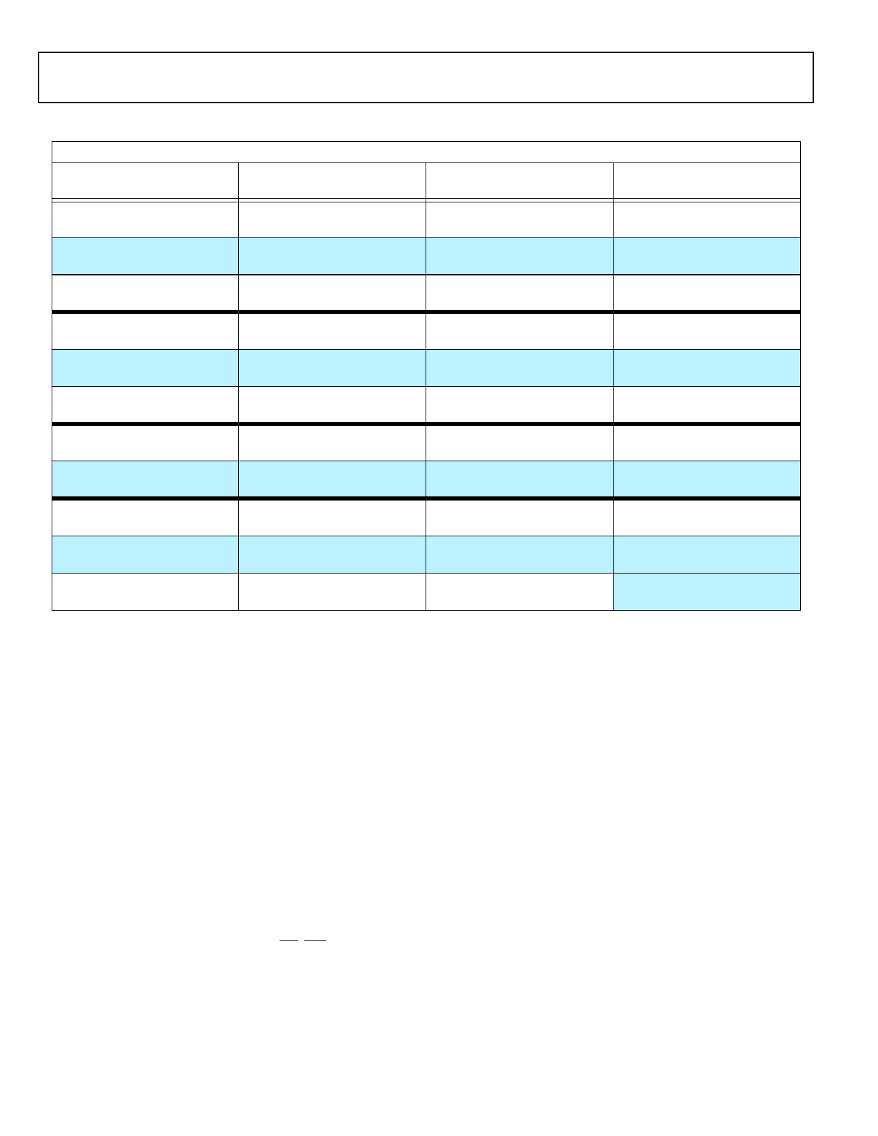
Table 3. ADSP-2136x Internal Memory Space
IOP Registers 0x0000 0000–0003 FFFF
Long Word (64 Bits)
Extended Precision Normal or
Instruction Word (48 Bits) Normal Word (32 Bits)
BLOCK 0 ROM
0x0004 0000–0x0004 7FFF
BLOCK 0 ROM
0x0008 0000–0x0008 AAA9
BLOCK 0 ROM
0x0008 0000–0x0008 FFFF
Reserved
0x0004 8000–0x0004 BFFF
Reserved
0x0009 0000–0x0009 7FFF
BLOCK 0 SRAM
0x0004 C000–0x0004 FFFF
BLOCK 0 SRAM
0x0009 0000–0x0009 5554
BLOCK 0 SRAM
0x0009 8000–0x0009 FFFF
BLOCK 1 ROM
0x0005 0000–0x0005 7FFF
BLOCK 1 ROM
0x000A 0000–0x000A AAA9
BLOCK 1 ROM
0x000A 0000–0x000A FFFF
Reserved
0x0005 8000–0x0005 BFFF
Reserved
0x000B 0000–0x000B 7FFF
BLOCK 1 SRAM
0x0005 C000–0x0005 FFFF
BLOCK 1 SRAM
0x000B 0000–0x000B 5554
BLOCK 1 SRAM
0x000B 8000–0x000B FFFF
BLOCK 2 SRAM
0x0006 0000–0x0006 1FFF
BLOCK 2 SRAM
0x000C 0000–0x000C 2AA9
BLOCK 2 SRAM
0x000C 0000–0x000C 3FFF
Reserved
0x0006 2000–0x0006 FFFF
Reserved
0x000C 4000–0x000D FFFF
BLOCK 3 SRAM
0x0007 0000–0x0007 1FFF
BLOCK 3 SRAM
0x000E 0000–0x000E 2AA9
BLOCK 3 SRAM
0x000E 0000–0x000E 3FFF
Short Word (16 Bits)
BLOCK 0 ROM
0x0010 0000–0x0011 FFFF
Reserved
0x0012 0000–0x0012 FFFF
BLOCK 0 SRAM
0x0013 0000–0x0013 FFFF
BLOCK 1 ROM
0x0014 0000–0x0015 FFFF
Reserved
0x0016 0000–0x0016 FFFF
BLOCK 1 SRAM
0x0017 0000–0x0017 FFFF
BLOCK 2 SRAM
0x0018 0000–0x0018 7FFF
Reserved
0x0018 8000–0x001B FFFF
BLOCK 3 SRAM
0x001C 0000–0x001C 7FFF
Rev. A | Page 6 of 52 | December 2006
Share Link: 