ADF4193(RevB) 데이터 시트보기 (PDF) - Analog Devices
부품명
상세내역
일치하는 목록
ADF4193 Datasheet PDF : 28 Pages
| |||
ADF4193
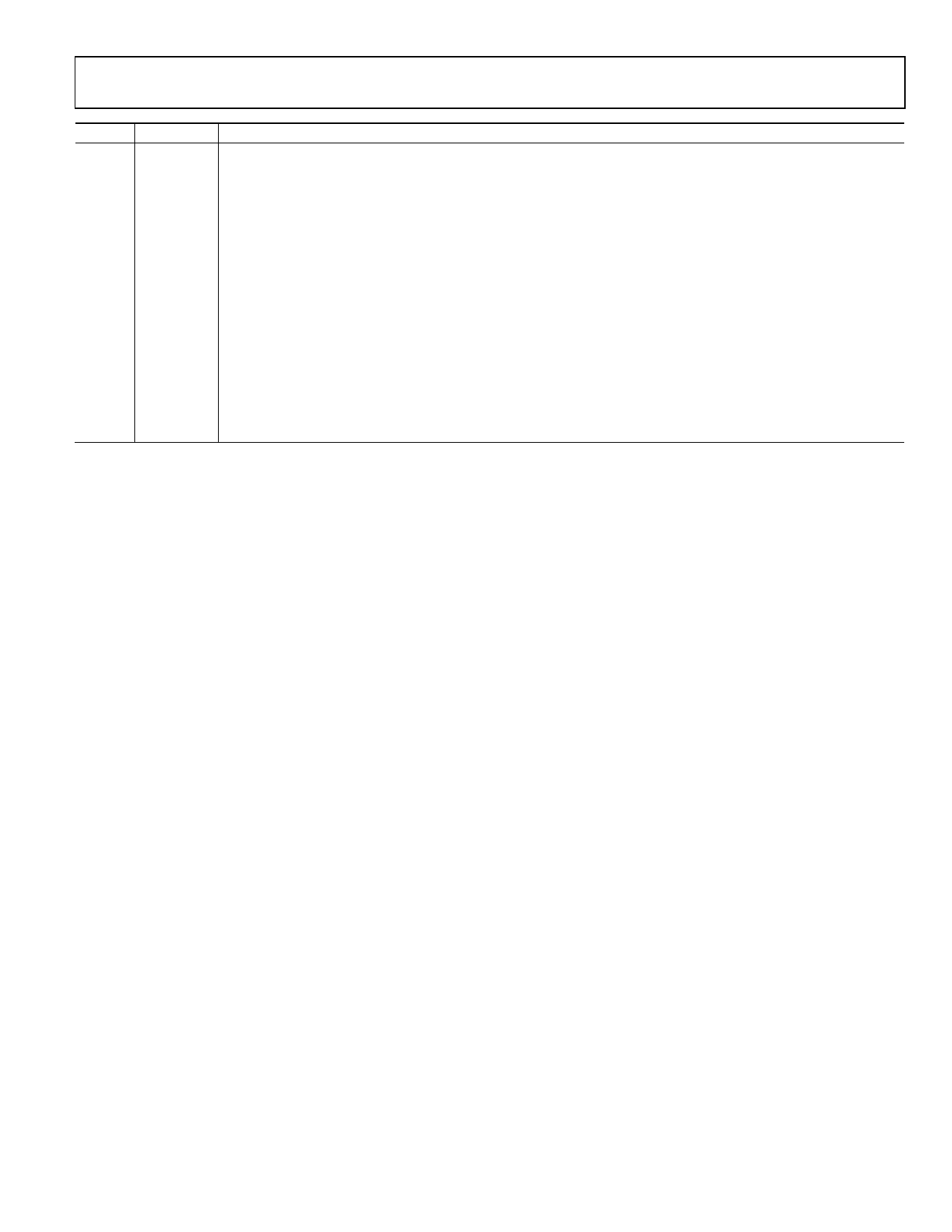
Pin No.
23
24
25
26
27
28
29
30
31
32
Mnemonic
RSET
VP2
AIN−
CPOUT−
SW2
SWGND
SW1
CPOUT+
AIN+
VP3
Description
Connecting a resistor between this pin and GND sets the charge pump output current. The nominal voltage bias at
the RSET pin is 0.55 V. The relationship between ICP and RSET is
ICP = 0.25/RSET
So, with RSET = 2.4 kΩ, ICP = 104 μA.
Power Supply Pin for the Charge Pump. Nominally 5 V, should be at the same voltage at VP1. A 0.1 μF decoupling
capacitor to ground should be placed as close as possible to this pin.
Differential Amplifier’s Negative Input Pin.
Differential Charge Pump’s Negative Output Pin. Should be connected to AIN− and the loop filter.
Fast Lock Switch 2. This switch is closed to SWGND while the SW1/2 timeout counter is active.
Common for SW1 and SW2 Switches. Should be connected to the ground plane.
Fast Lock Switch 1. This switch is closed to SWGND while the SW1/2 timeout counter is active.
Differential Charge Pump’s Positive Output Pin. Should be connected to AIN+ and the loop filter.
Differential Amplifier’s Positive Input Pin.
Power Supply Pin for the Differential Amplifier. This can range from 5.0 V to 5.5 V. A 0.1 μF decoupling capacitor to
ground should be placed as close as possible to this pin. Also requires a 10 μF decoupling capacitor to ground.
Rev. B | Page 7 of 28
Share Link: 