AD9725 데이터 시트보기 (PDF) - Analog Devices
부품명
상세내역
일치하는 목록
AD9725 Datasheet PDF : 16 Pages
| |||
Preliminary Technical Data
AD9725
DIGITAL SPECIFICATIONS
Table 3. TMIN to TMAX, AVDD1, AVDD2, DBVDD = 3.3 V, ADVDD, ACVDD, CLKVDD, DVDD = 2.5 V , IOUTFS = 20 mA, unless
otherwise noted. Specifications subject to change without notice.
Parameter
Conditions
Min
Typ Max Unit
Digital Inputs
VCM = 0.875 V to 1.575 V
Differential Logic ‘1’
(put into footnote, and delete 0.1
column?)
0.6
V
Differential Logic ‘0’
–0.6
–0.1 V
Logic ‘1’ current
3.5
mA
Logic ‘0’ current
3.5
mA
Differential Input Resistance
100
W
Differential Input Capacitance
3
pF
Data Setup Time (tDS)
0.9
ns
Data Hold Time (tDH)
–0.3
ns
Data Clock Output Delay ( tDCO)
2.4
ns
Serial Control Bus
Maximum SCLK Frequency (fSCLK)
15
MHz
Minimum Clock Pulse Width High (tPWH)
30
ns
Minimum Clock Pulse Width Low (tPWL)
30
ns
Maximum Clock Rise/Fall Time
1
ms
Minimum Data/Chip Select Set Up Time (tDS)
25
ns
Minimum Data Hold Time (tDH)
0
ns
Maximum Data Valid Time (tDV)
30
ns
RESET Pulse Width
1.5
ns
Inputs (SDI, SDIO, SCLK, CSB)
Logic ‘1’ Voltage
2.1
3
V
Logic ‘0’ Voltage
0
0.9
V
Logic ‘1’ Current
–10
+10 µA
Logic ‘0’ Current
–10
+10 µA
Input Capacitance
5
pF
SDIO Output
Logic ‘1’ Voltage
DRVDD–0.6
V
Logic ‘0’ Voltage
0.4
V
Logic ‘1’ Current
30
50
mA
Logic ‘0’ Current
30
50
mA
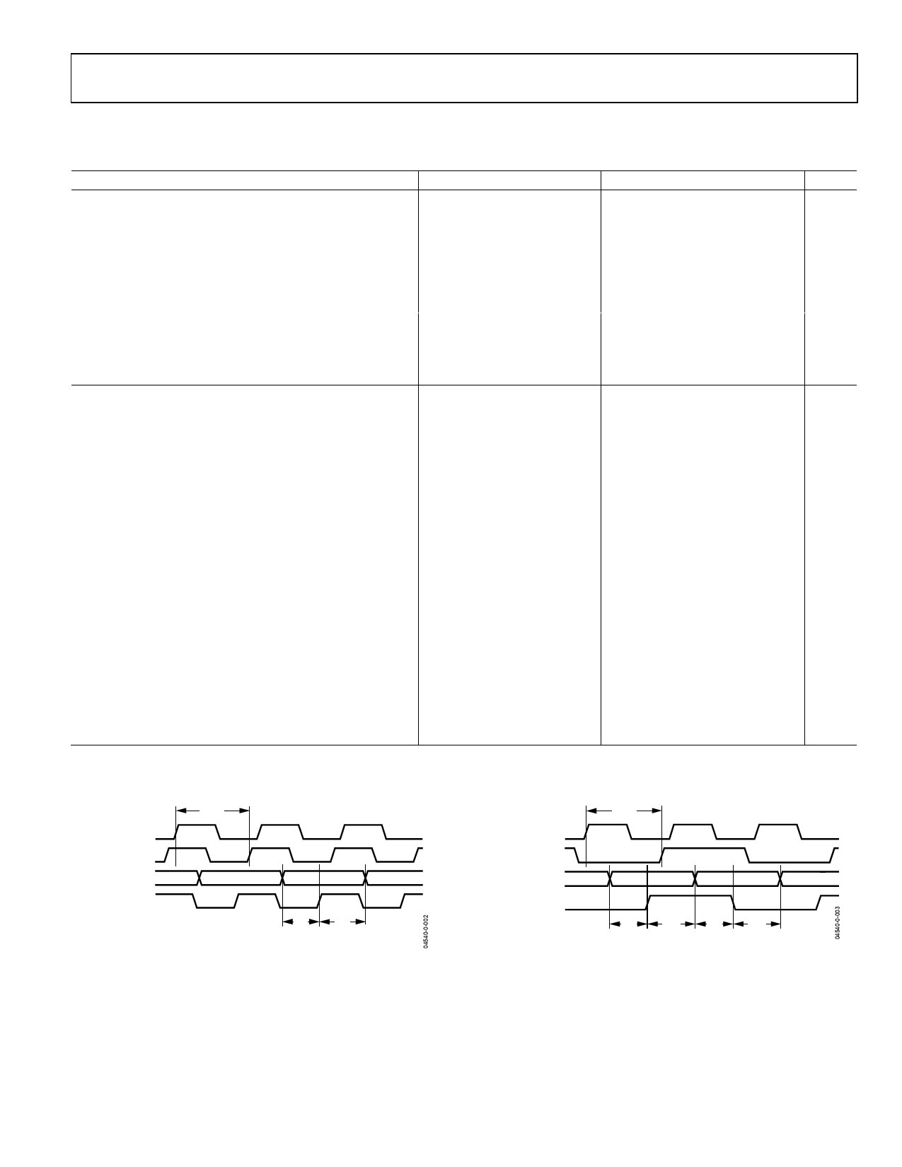
DIGITAL TIMING INFORMATION
tDCO
CLK
DATACLK_OUT
DB[15:0]
DATACLK_IN
tDS
tDH
Figure 2. Single Datarate (SDR) Mode
CLK
DATACLK_OUT
DB[15:0]
DATACLK_IN
tDCO
tDS
tDH
tDS
tDH
Figure 3. Double Datarate (DDR) Mode
Rev. PrA | Page 5 of 16
Share Link: 