AD9230-210 데이터 시트보기 (PDF) - Analog Devices
부품명
상세내역
일치하는 목록
AD9230-210 Datasheet PDF : 21 Pages
| |||
AD9230
Preliminary Technical Data
SWITCHING SPECIFICATIONS
Table 4. (AVDD = 1.8 V, DRVDD = 1.8 V, TMIN = –40°C, TMAX = +85°C, DCS Enabled unless otherwise noted.)
AD9230-170/-210
AD9230-250
Parameter (Conditions)
Temp Min
Typ
Max
Min
Typ
Max
Maximum Conversion Rate1
Full 170/210
250
Minimum Conversion Rate1
Full
40
40
CLK+ Pulsewidth High (tEH)1
Full TBD
TBD
CLK+ Pulsewidth Low (tEL)1
Full TBD
TBD
OUTPUT (LVDS)
Valid Time (tV)
Full TBD
TBD
Propagation Delay (tPD)
Full
3.9
3.9
Rise Time (tR) (20% to 80%)
25°C
0.4
0.4
Fall Time (tF) (20% to 80%)
25°C
0.4
0.4
DCO Propagation Delay (tCPD) Full
3.2
3.2
Data to DCO Skew (tPD– tCPD)
Full
TBD
TBD
Latency
Full
5
5
Aperture Delay (tA)
25°C
Aperture Uncertainty (Jitter, tJ) 25°C
Out of Range Recovery Time
25°C
TBD
0.2
TBD
TBD
0.2
TBD
Unit
MSPS
MSPS
ns
ns
ns
ns
ns
ns
ns
ns
Cycles
ns
ps rms
Cycles
1 All ac specifications tested by driving CLK+ and CLK– differentially.
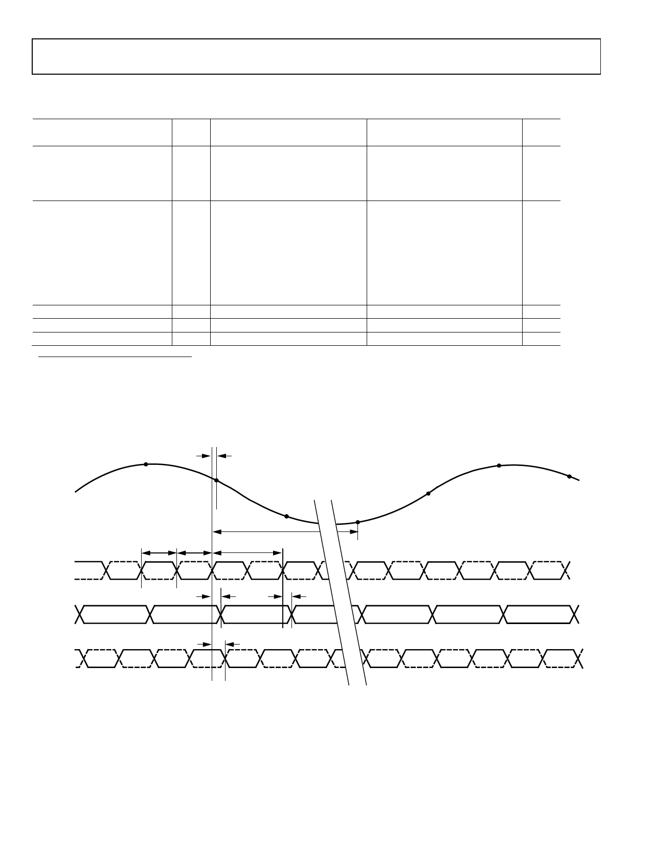
AIN
CLK+
CLK–
DATA
OUT
DCO+
DCO–
N–1
tA
N
tEH
tEL
N+1
L CYCLES
1/fS
N+L+1
N+L
N+L+2
N+L+3
tPD
tV
N–L
N-L+1
N
N+1
N+2
tCPD
Figure 2. Timing Diagram (L=5 Cycles)
Rev. PrE | Page 6 of 21
Share Link: 